A correct version of the HLK-10M05 is available here:
(before making new parts always do a google search of the form “fritzing part HLK-10M05”)
I’ll look over your HLK-30M12C part and correct it as needed.
edit:
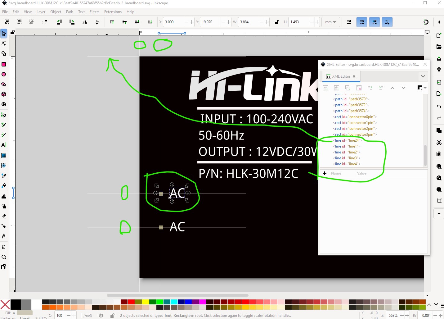
OK a number of corrections starting with breadboard
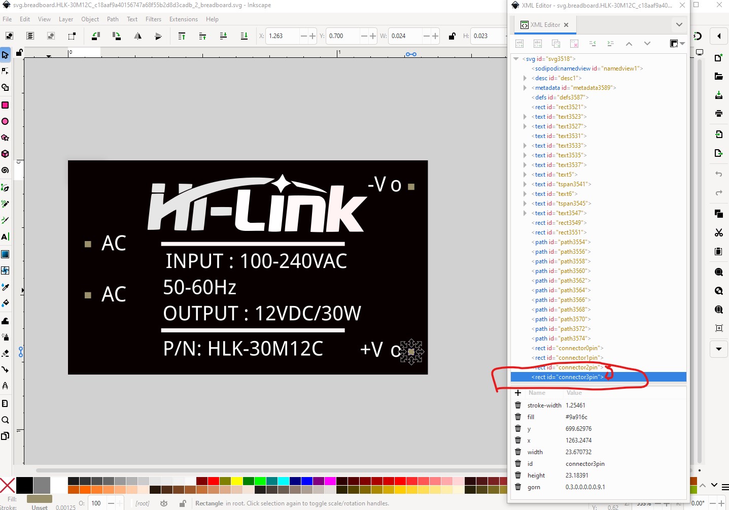
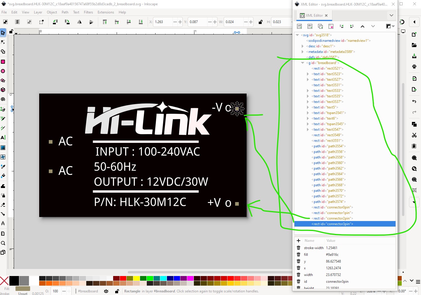
The output pin numbers are backwards connector2 wants to be on the bottom and connector3 on the top (the same format as an IC) so the two right pins need to swap pin numbers.
you are missing a layerId which will cause the part to not export as an image (and get questions as to why that is!)
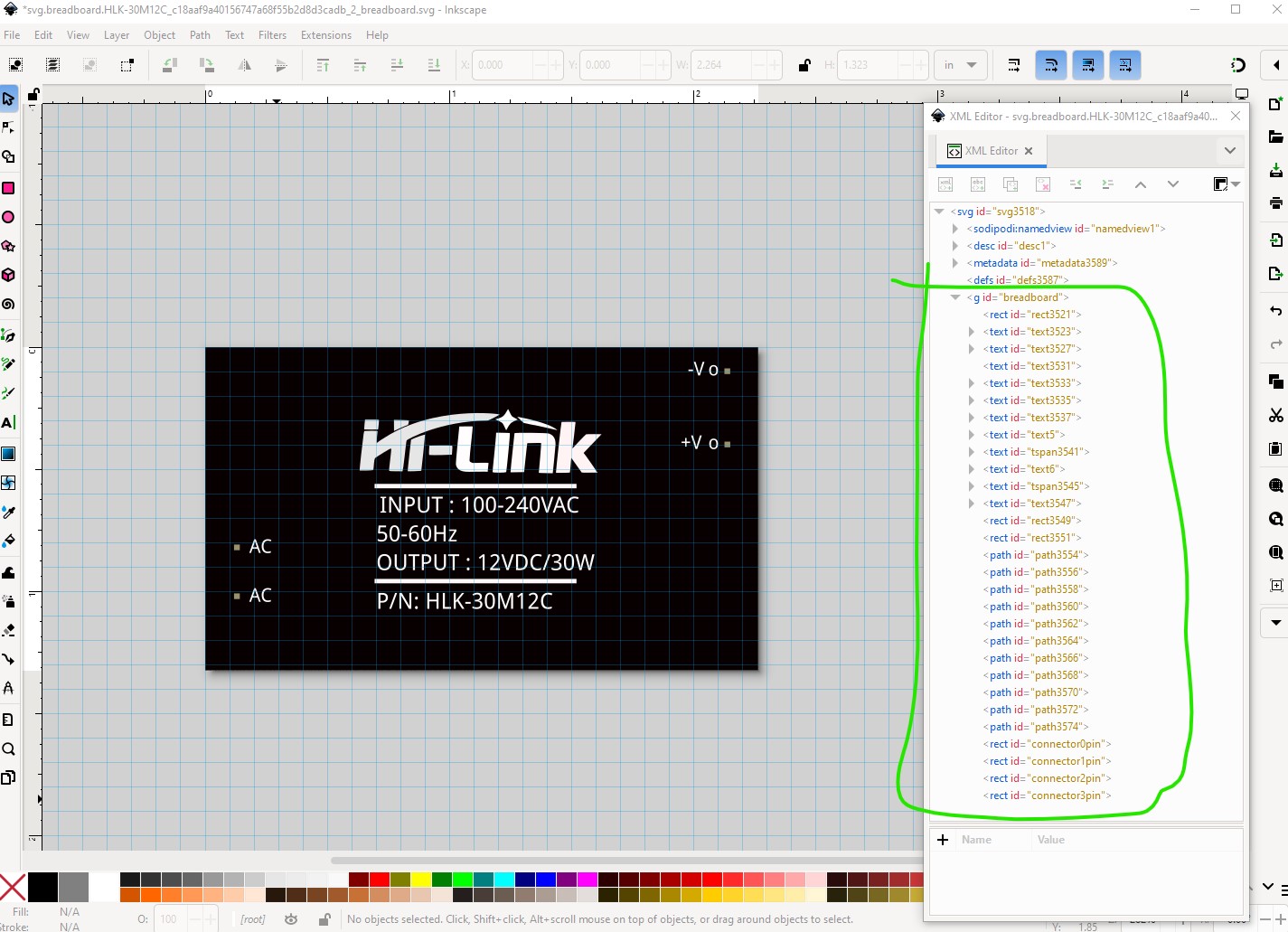
from the data sheet
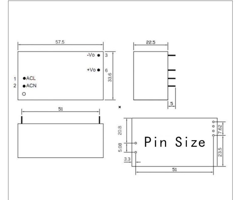
the breadboard image is the wrong size and the pins are in the wrong position (both are supposed to reflect real life)
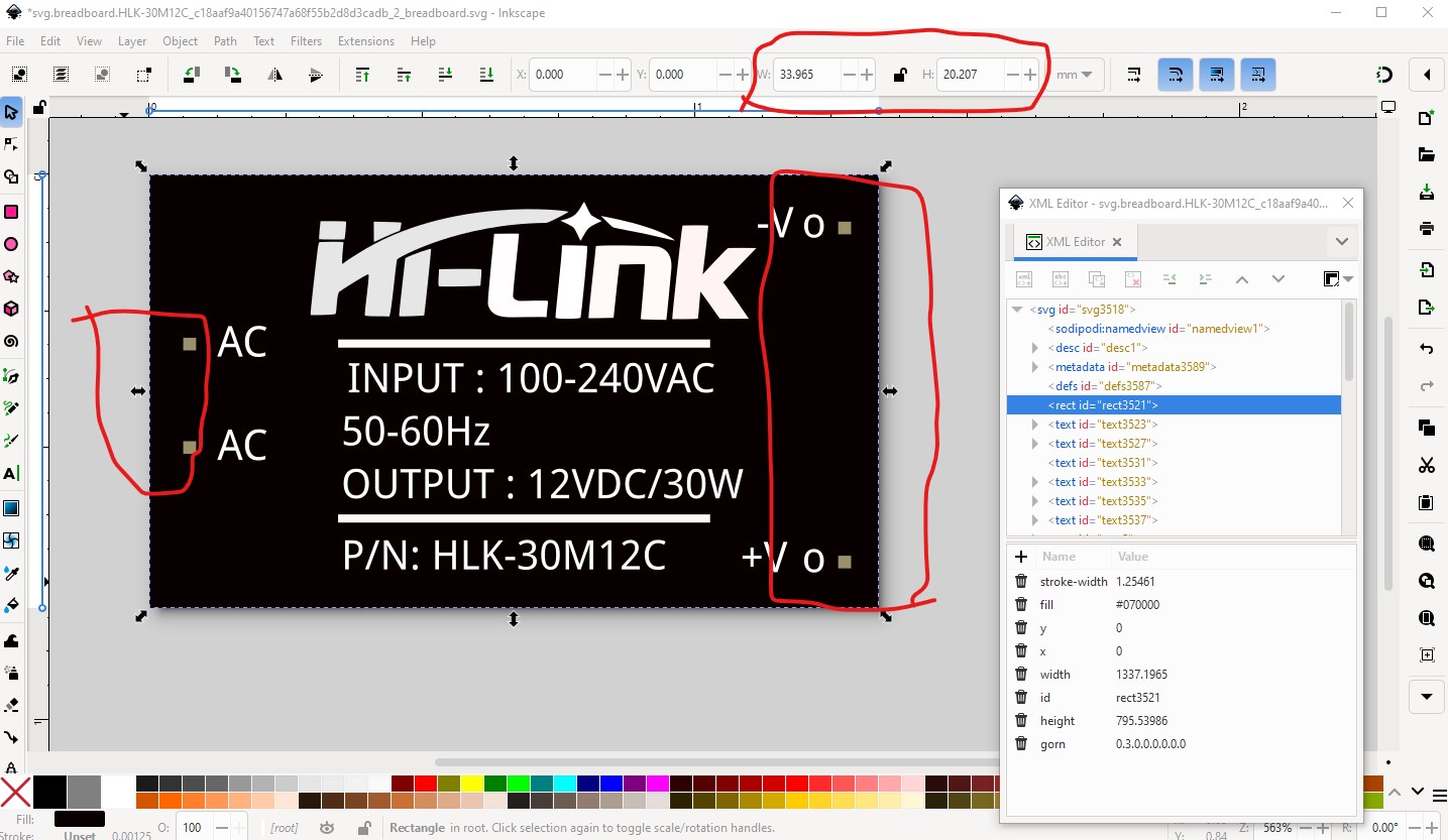
from the data sheet I set construction lines (after resizing the rectangle to the correct size) to mark the position of the pins then moved them to where they should be.
Then I did an Edit->select all an Edit->Resize page to selection and Object->group and named the group breadboard (which is what it is called in the .fzp file) then saved the corrected svg.
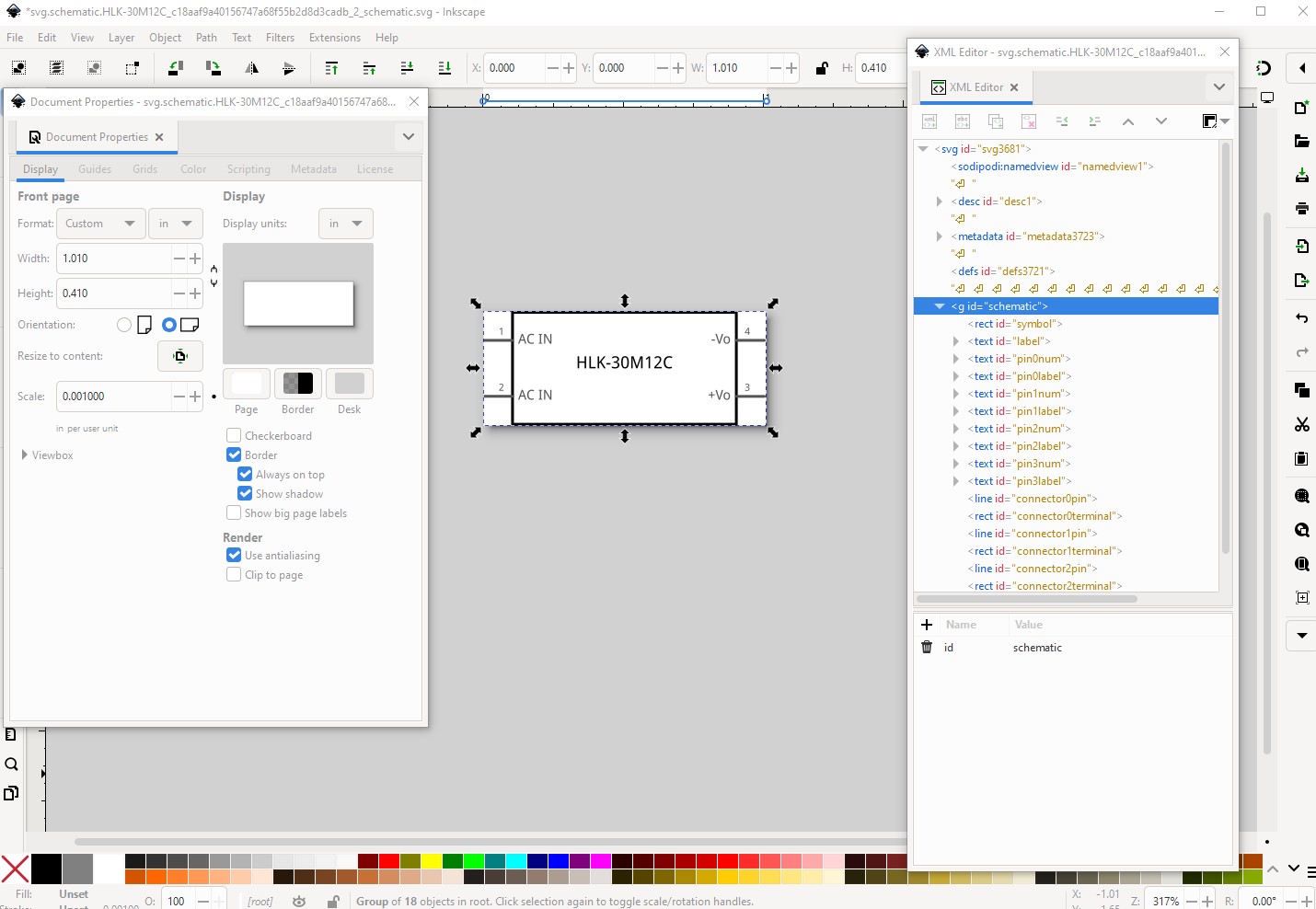
schematic has a number of problems
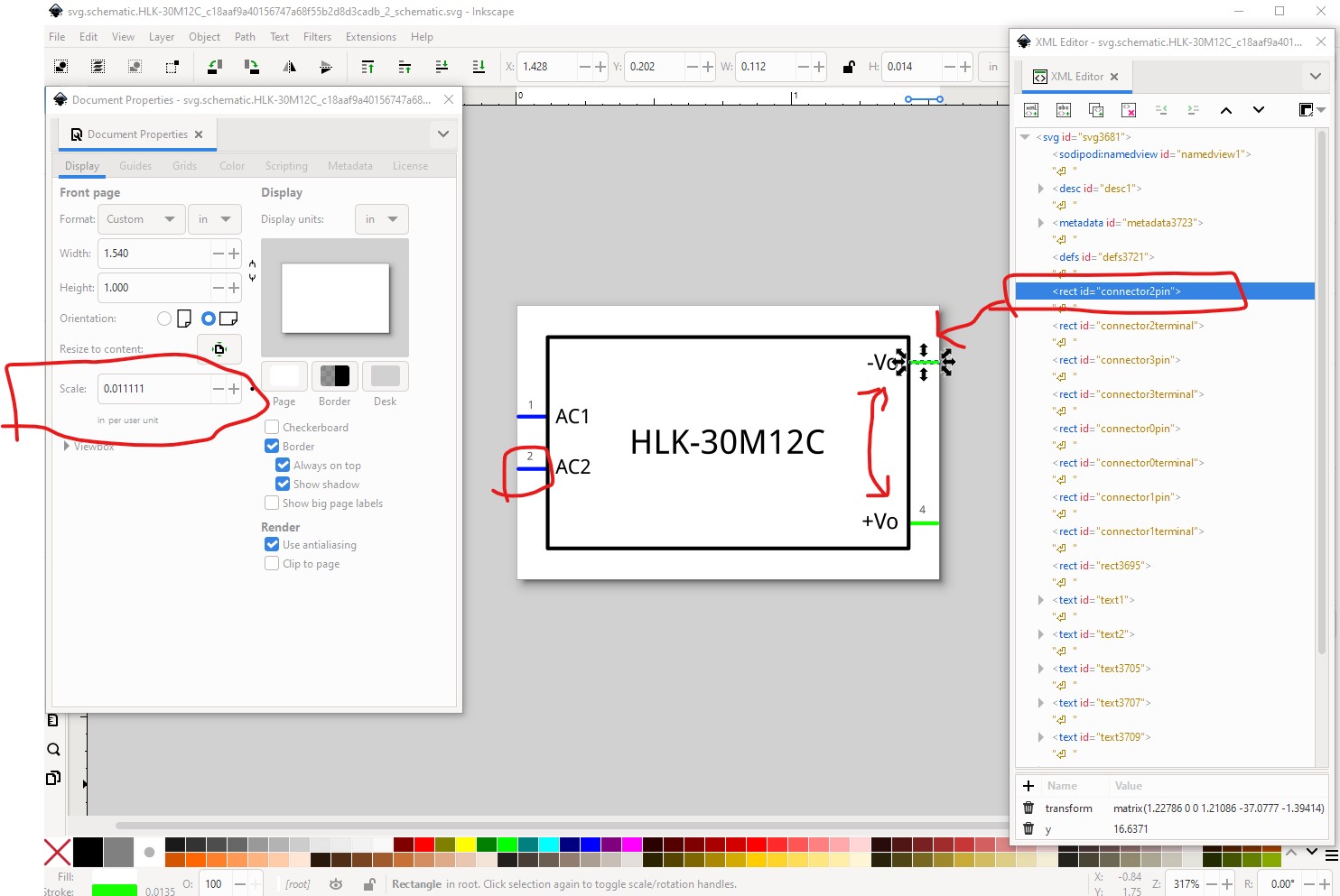
It doesn’t have the correct scale nor the correct colors or font sizes. Rather than try and fix it I chose to make a new schematic using Randy’s Inkscape fritzing schematic extension
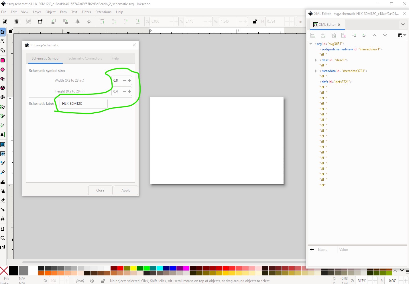

then set the pin names for the first 2 pins
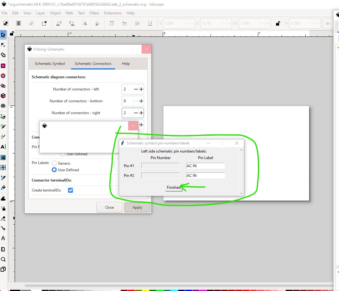
then the last 2 pins
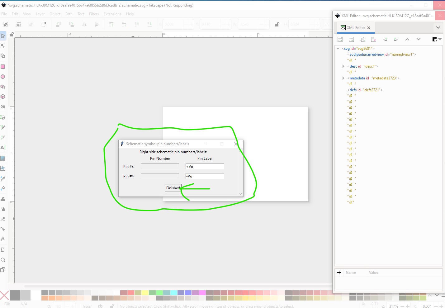
and hit finished and it creates the new svg at the correct scale with the correct layerId
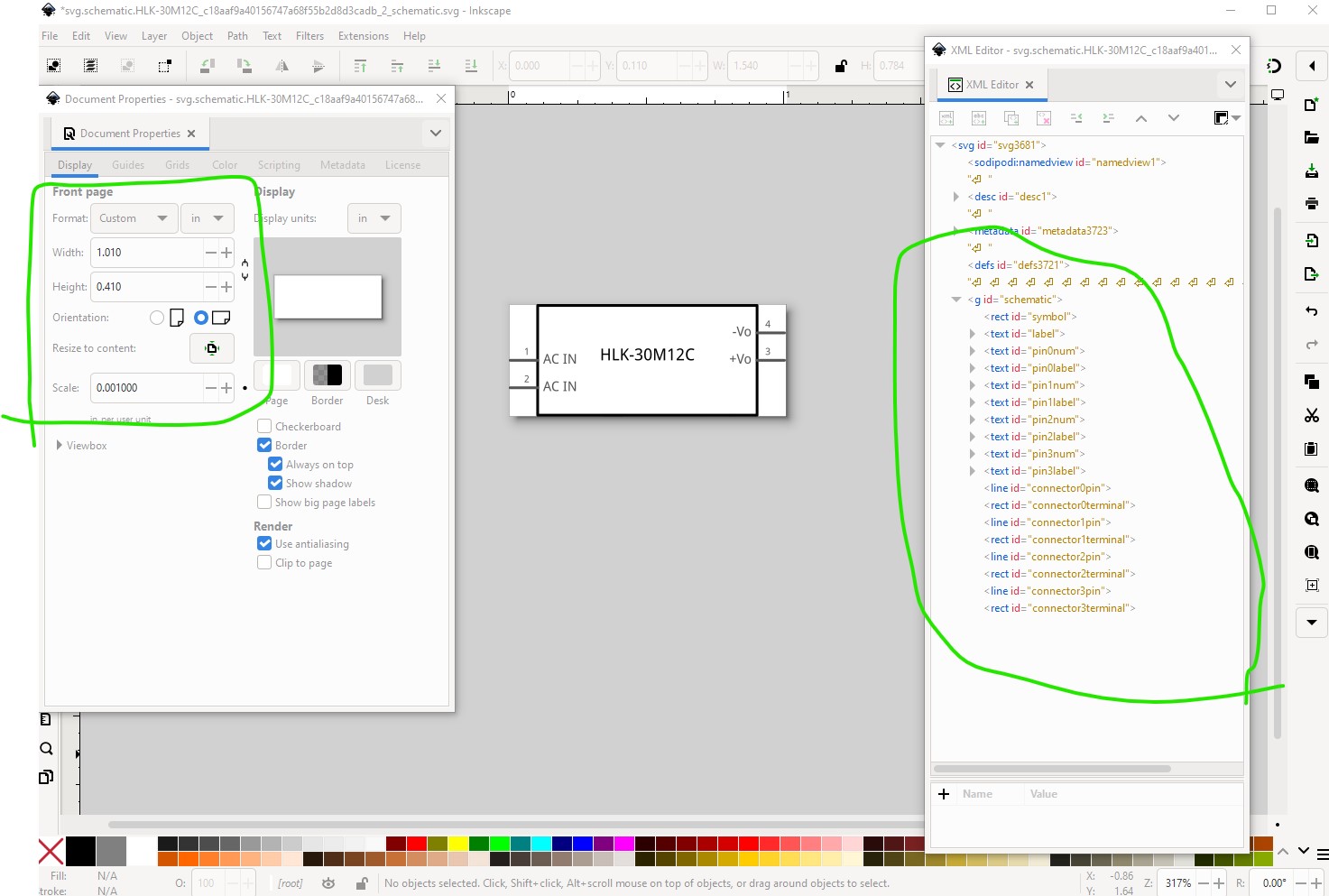
however the pins are slightly offset so ungroup the svg and then move the pins in to a better position and then regroup the svg and set the layerId again
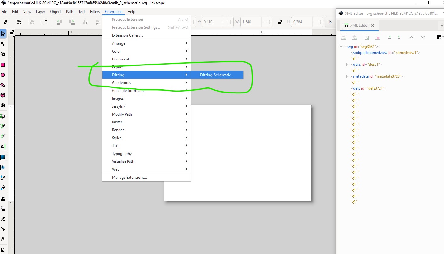
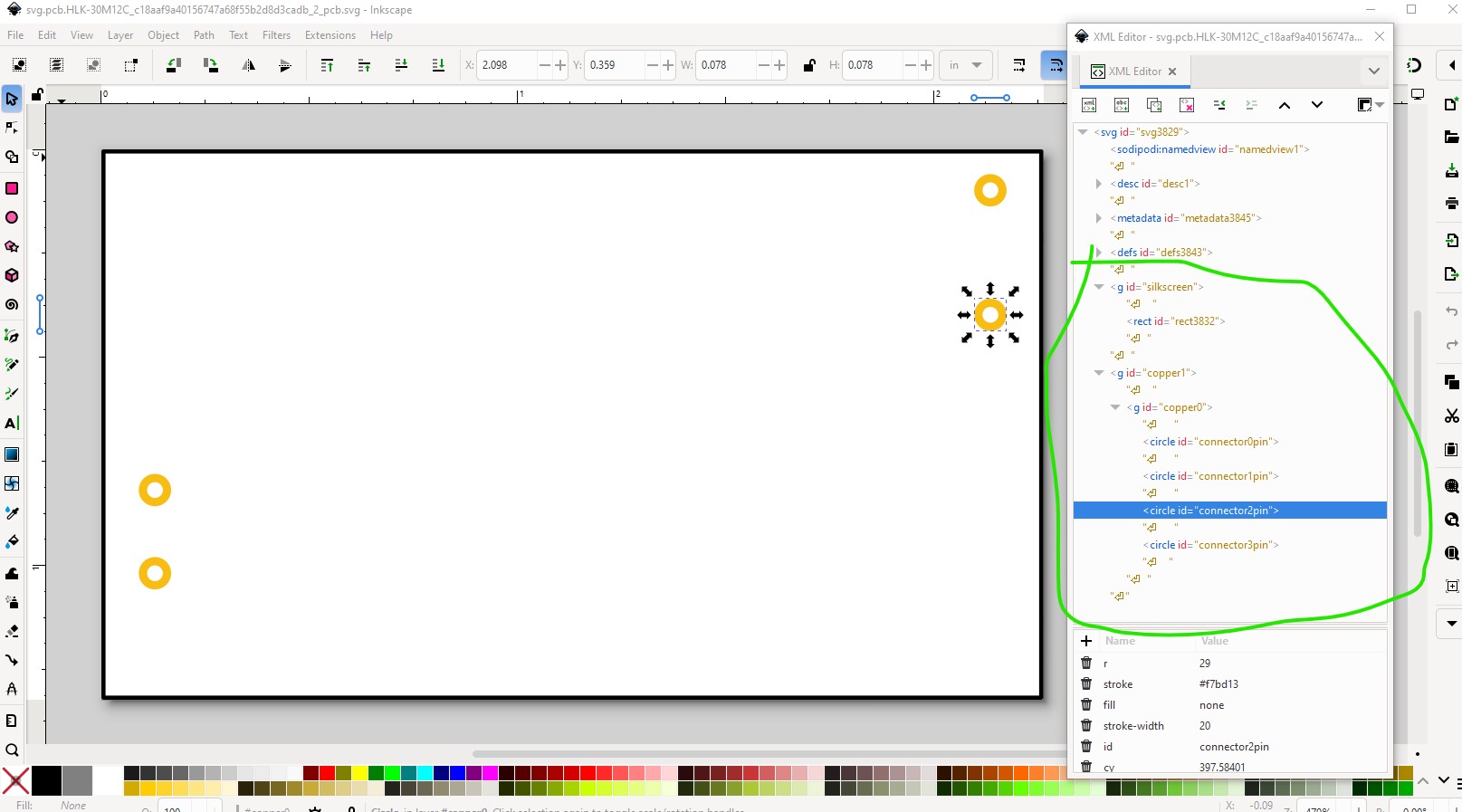
then save the svg and move on to pcb there are a couple of problems here, the pin numbers need to be corrected to reflect the numbers used in breadboard and schematic, and the pins need to be circles (not ellipses as they are now, ellipses will not generate a hole in the gerber output!)
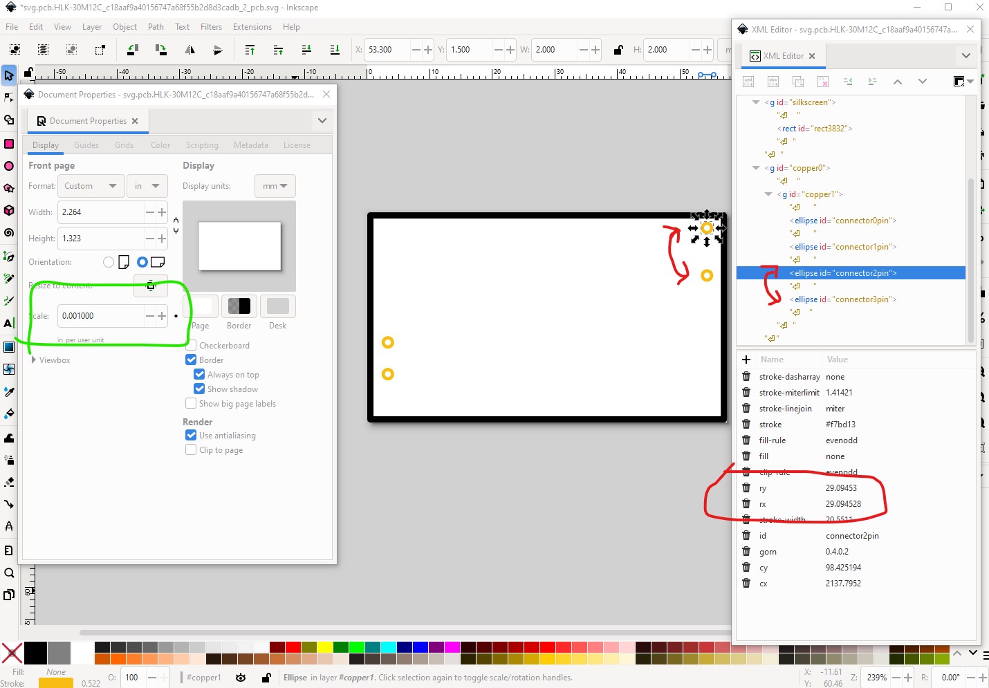
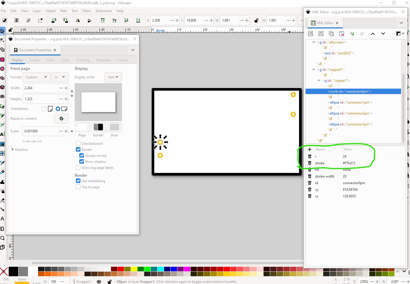
the easiest way to correct the radius is set both 4x and ry in xml editor to the same value (I used a radius of 29 which will give a 0.038 hole suitable for a 0.1in header)
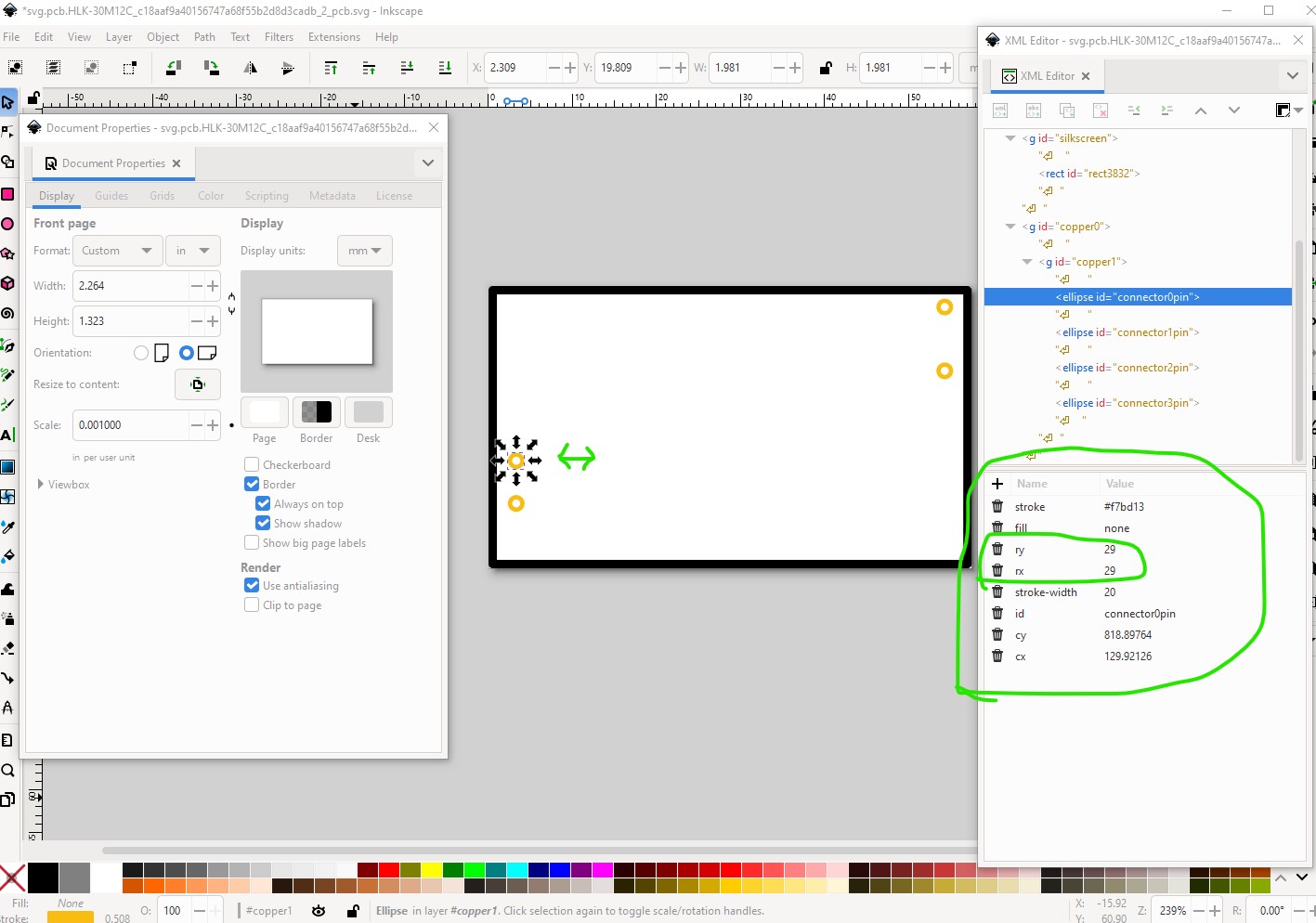
then move the pad on space left then one space right to put it back in the same position it was. Inkscape recognizes that the ellipse has changed to a circle and replaces rx and ry with r=29 which along with a stroke-width of 20 will produce the correct hole size like this
next we need to change the stroke-width of the silkscreen rectangle to 10 (to make it 10thou inches which is the standard silkscreen line size.)
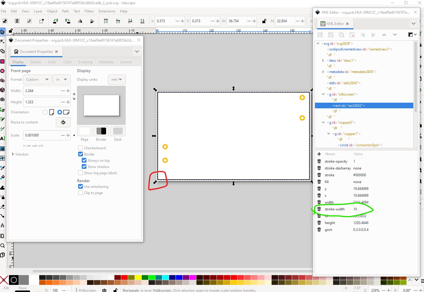
That changes the size of the rectangle slightly so we need to first correct that
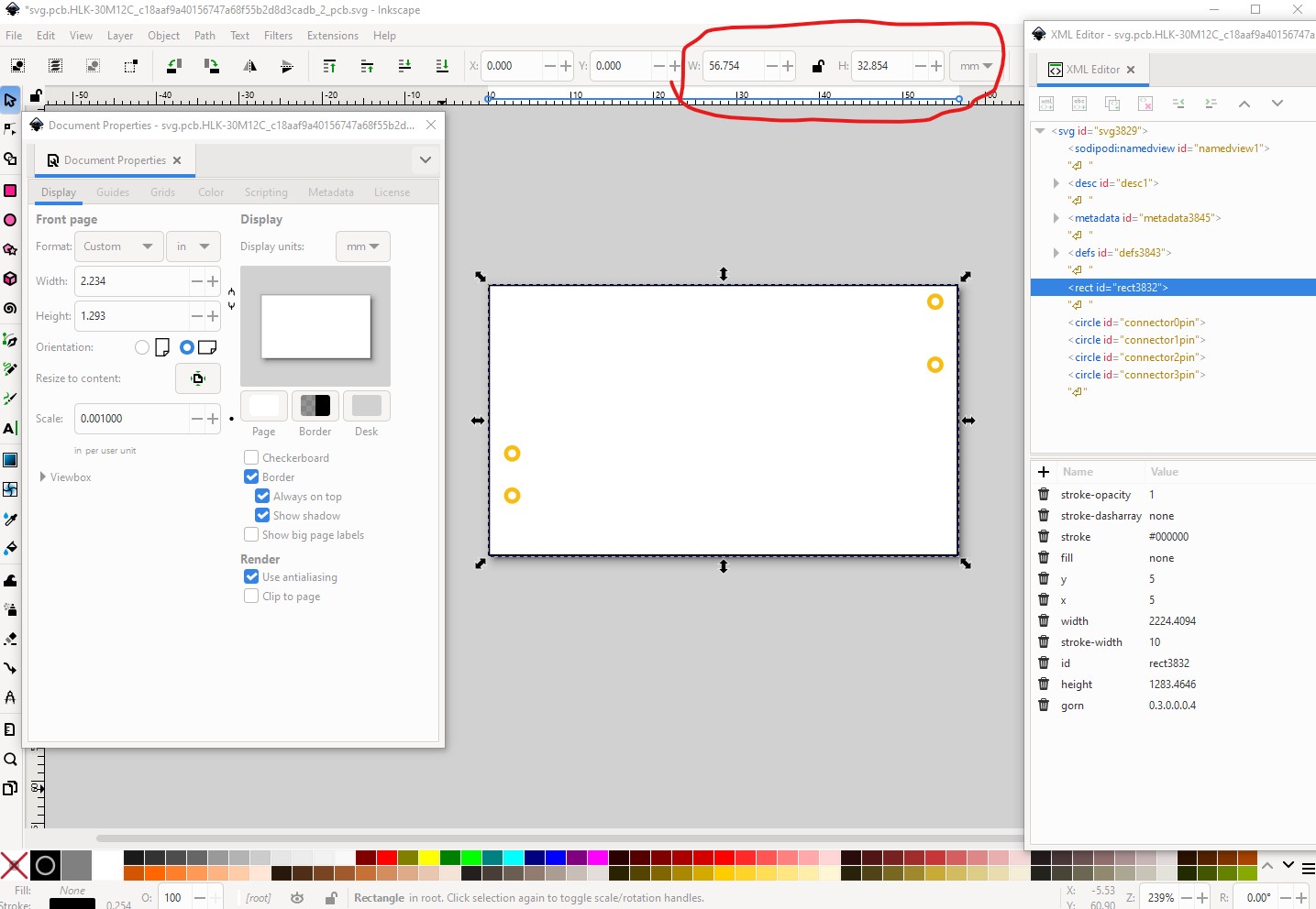
then change the width and height to match the data sheet then set up the construction lines to correctly move the pads in the correct position (they were already in the correct position before I changed the rectangle size, so the entire group only needed to be moved to the correct new position.)

re doing the groups creates the completed pcb svg which can now be saved.
On to the .fzp file
<module fritzingVersion="1.0.5" moduleId="HLK-30M12C_c18aaf9a40156747a68f55b2d8d3cadb_1" referenceFile="generic_ic_dip_4_300mil.fzp">
I updated the fritzing version to the version I tested the part on (1.0.5) and then
  <author>Iyad Nahas (modified by vanepp May 2025)</author>
  <title>HLK-30M12C</title>
  <label>A</label>
updated the author field to say I modified your part, corrected the title to reflect the correct part number and set the label to A (for assumbly) then I updated the label property to reflect the correct part number
<property name="label">HLK-30M12C</property>
corrected the description field to match the voltage output of the new part
<description><!DOCTYPE HTML PUBLIC "-//W3C//DTD HTML 4.0//EN" "http://www.w3.org/TR/REC-html40/strict.dtd">
<html><head><meta name="qrichtext" content="1" /><style type="text/css">
p, li { white-space: pre-wrap; }
</style></head><body style=" font-family:'.SF NS Text'; font-size:13pt; font-weight:400; font-style:normal;">
<p style=" margin-top:0px; margin-bottom:0px; margin-left:0px; margin-right:0px; -qt-block-indent:0; text-indent:0px;">AC-DC 220V to 12V Step-Down Power Supply Module</p></body></html></description>
reused the breadboard svg as the icon svg (to save file space)
    <iconView>
      <layers image="breadboard/HLK-30M12C_c18aaf9a40156747a68f55b2d8d3cadb_2_breadboard.svg">
        <layer layerId="icon"/>
      </layers>
    </iconView>
then changed the description and name fields in connectors2 and connector3 to reflect the new order of the two pins by reversing connectors 2 and 3.
    <connector id="connector2" name="+Vo" type="male">
      <description>+V Out</description>
      <views>
        <breadboardView>
          <p layer="breadboard" svgId="connector2pin"/>
        </breadboardView>
        <schematicView>
          <p layer="schematic" svgId="connector2pin" terminalId="connector2terminal"/>
        </schematicView>
        <pcbView>
          <p layer="copper0" svgId="connector2pin"/>
          <p layer="copper1" svgId="connector2pin"/>
        </pcbView>
      </views>
    </connector>
    <connector id="connector3" name="-Vo" type="male">
      <description>-V Out</description>
      <views>
        <breadboardView>
          <p layer="breadboard" svgId="connector3pin"/>
        </breadboardView>
        <schematicView>
          <p layer="schematic" svgId="connector3pin" terminalId="connector3terminal"/>
        </schematicView>
        <pcbView>
          <p layer="copper0" svgId="connector3pin"/>
          <p layer="copper1" svgId="connector3pin"/>
        </pcbView>
      </views>
    </connector>
then corrected the url field to point to the datasheet for this part
<url>https://www.lcsc.com/datasheet/lcsc_datasheet_2409141607_HI-LINK-HLK-30M12_C2761166.pdf</url>
which creates this corrected part.
HLK-30M12C-fixed.fzpz (7.1 KB)
which should do what you want.
Peter