I ran your part through FritzingCheckPart.py and it has a number of complaints.
“This is a through hole part as both copper0 and copper1 views are present.
If you wanted a smd part remove the copper0 definition from line 47”
except this is a SMD part and thus copper0 should not be present.
"Warning 14: File
‘part.SK6812 Mini-E New_c1bf5d38d530ff2aaa36d248bd23d316_1.fzp.bak’
At line 104
terminalId missing in schematicView (likely an error)"
"Error 18: File
‘part.SK6812 Mini-E New_c1bf5d38d530ff2aaa36d248bd23d316_1.fzp.bak’
Connector connector0terminal is in the fzp file but not the svg file. (typo?)
svg svg.schematic.SK6812 Mini-E New_67d918244604ca65118d5cb1d23e9181_2_schematic.svg.bak
Error 18: File
‘part.SK6812 Mini-E New_c1bf5d38d530ff2aaa36d248bd23d316_1.fzp.bak’
Connector connector2terminal is in the fzp file but not the svg file. (typo?)
svg svg.schematic.SK6812 Mini-E New_67d918244604ca65118d5cb1d23e9181_2_schematic.svg.bak"
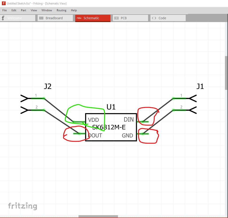
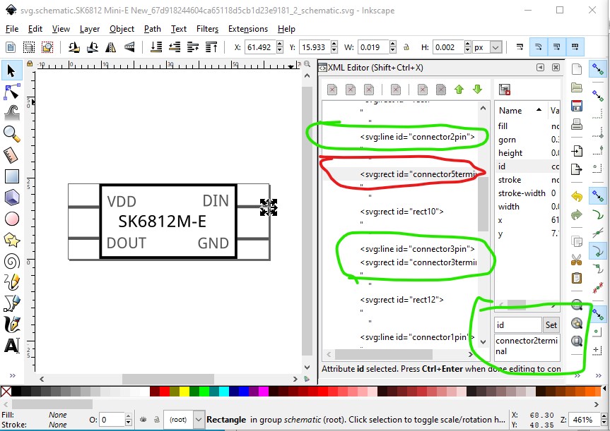
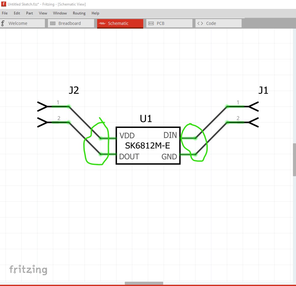
Which causes the red circles here in schematic. If the terminalId doesn’t exist Fritzing uses the center of the pin (which in this case is incorrect!) It appears pin1 has a terminalId as it is correct.
As well the alignment to the grid is off by a bit.
"Warning 19: File
‘svg.breadboard.SK6812 Mini-E New_67d918244604ca65118d5cb1d23e9181_2_breadboard.svg.bak’
At line 2
Height 15.507933 is defined in px
in or mm is a better option (px can cause scaling problems!)
Warning 19: File
‘svg.breadboard.SK6812 Mini-E New_67d918244604ca65118d5cb1d23e9181_2_breadboard.svg.bak’
At line 2
Width 23.5 is defined in px
in or mm is a better option (px can cause scaling problems!)"
As the message says, it is better to us in or mm as the units, px will cause Fritzing to guess between 72dpi, 90dpi or 96dpi and it often gets it wrong and the part’ scale is incorrect. That may or may not be happening here. Same is true in pcb
"Warning 19: File
‘svg.pcb.SK6812 Mini-E New_67d918244604ca65118d5cb1d23e9181_2_pcb.svg.bak’
At line 3
Height 13.815009 is defined in px
in or mm is a better option (px can cause scaling problems!)
Warning 19: File
‘svg.pcb.SK6812 Mini-E New_67d918244604ca65118d5cb1d23e9181_2_pcb.svg.bak’
At line 3
Width 31.195753 is defined in px
in or mm is a better option (px can cause scaling problems!)"
"Error 74: File
‘svg.pcb.SK6812 Mini-E New_67d918244604ca65118d5cb1d23e9181_2_pcb.svg.bak’
At line 43
Connector connector3pin has no radius no hole will be generated
Error 74: File
‘svg.pcb.SK6812 Mini-E New_67d918244604ca65118d5cb1d23e9181_2_pcb.svg.bak’
At line 44
Connector connector1pin has no radius no hole will be generated
Error 74: File
‘svg.pcb.SK6812 Mini-E New_67d918244604ca65118d5cb1d23e9181_2_pcb.svg.bak’
At line 45
Connector connector0pin has no radius no hole will be generated
Error 74: File
‘svg.pcb.SK6812 Mini-E New_67d918244604ca65118d5cb1d23e9181_2_pcb.svg.bak’
At line 46
Connector connector2pin has no radius no hole will be generated"
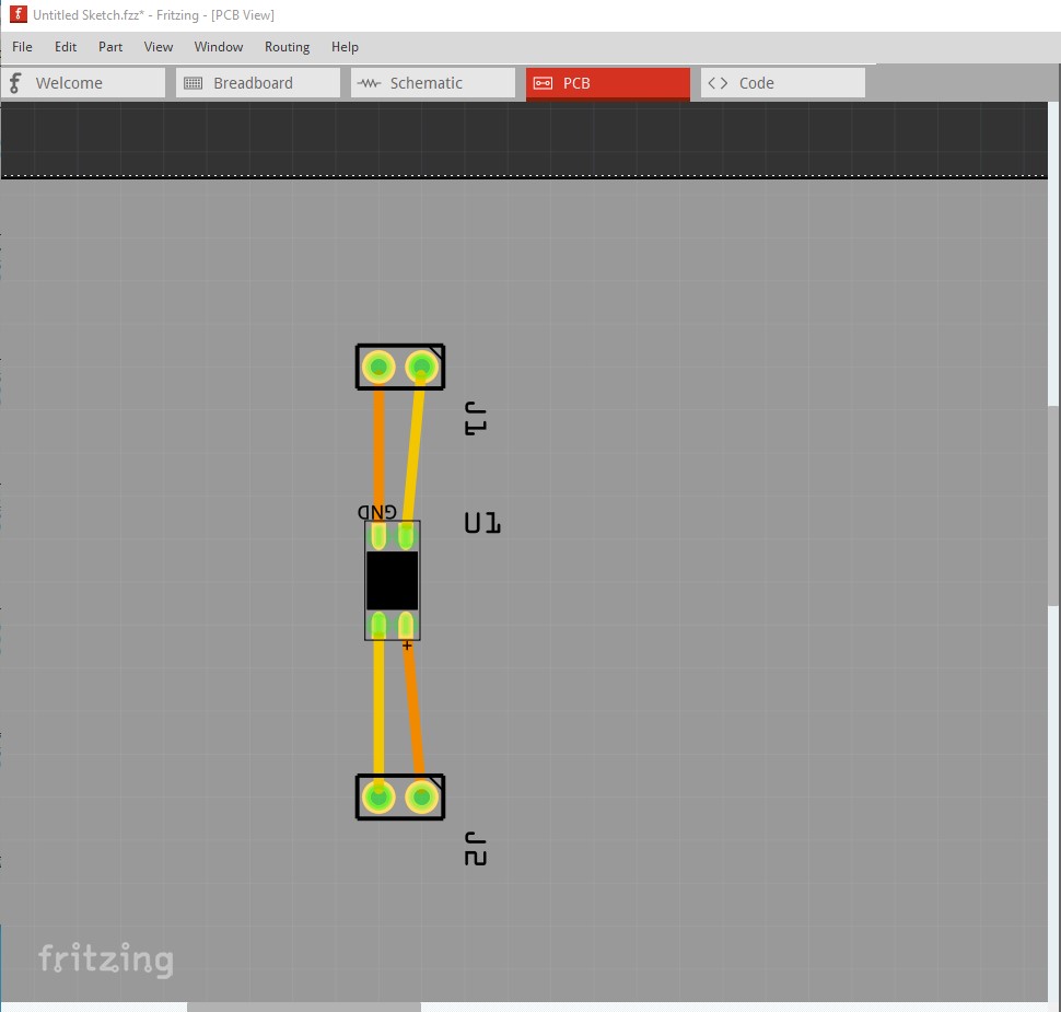
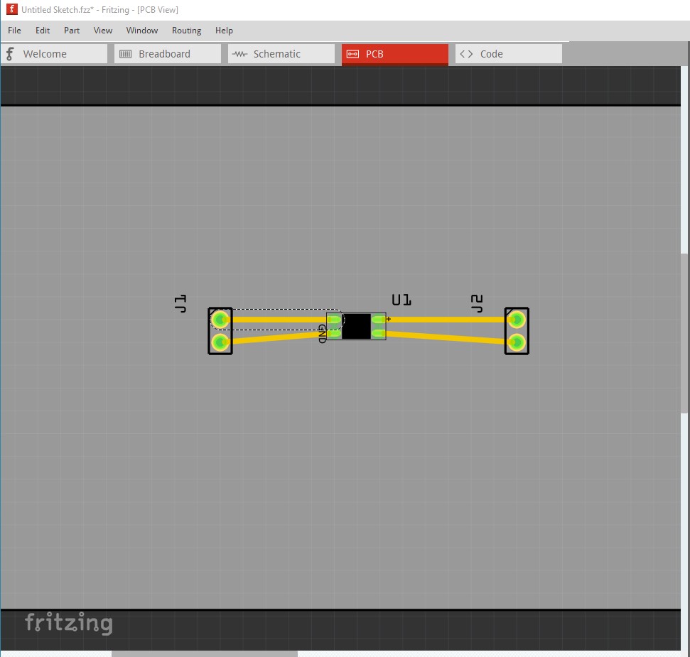
These 4 are complaining that the pads don’t have holes. Because this is a SMD part, they shouldn’t have holes, but Fritzing thinks this is a throuh hole part and will have put pads on both sides of the board. This may be what is confusing ground fill (or you may have hit a ground fill bug assuming you are running 0.9.6.) Here I dragged a couple of .1in headers in to the sketch and attached them on the top and bottom layers to your part (I shouldn’t be able to attach them on the bottom layer as this should be a SMD part.)
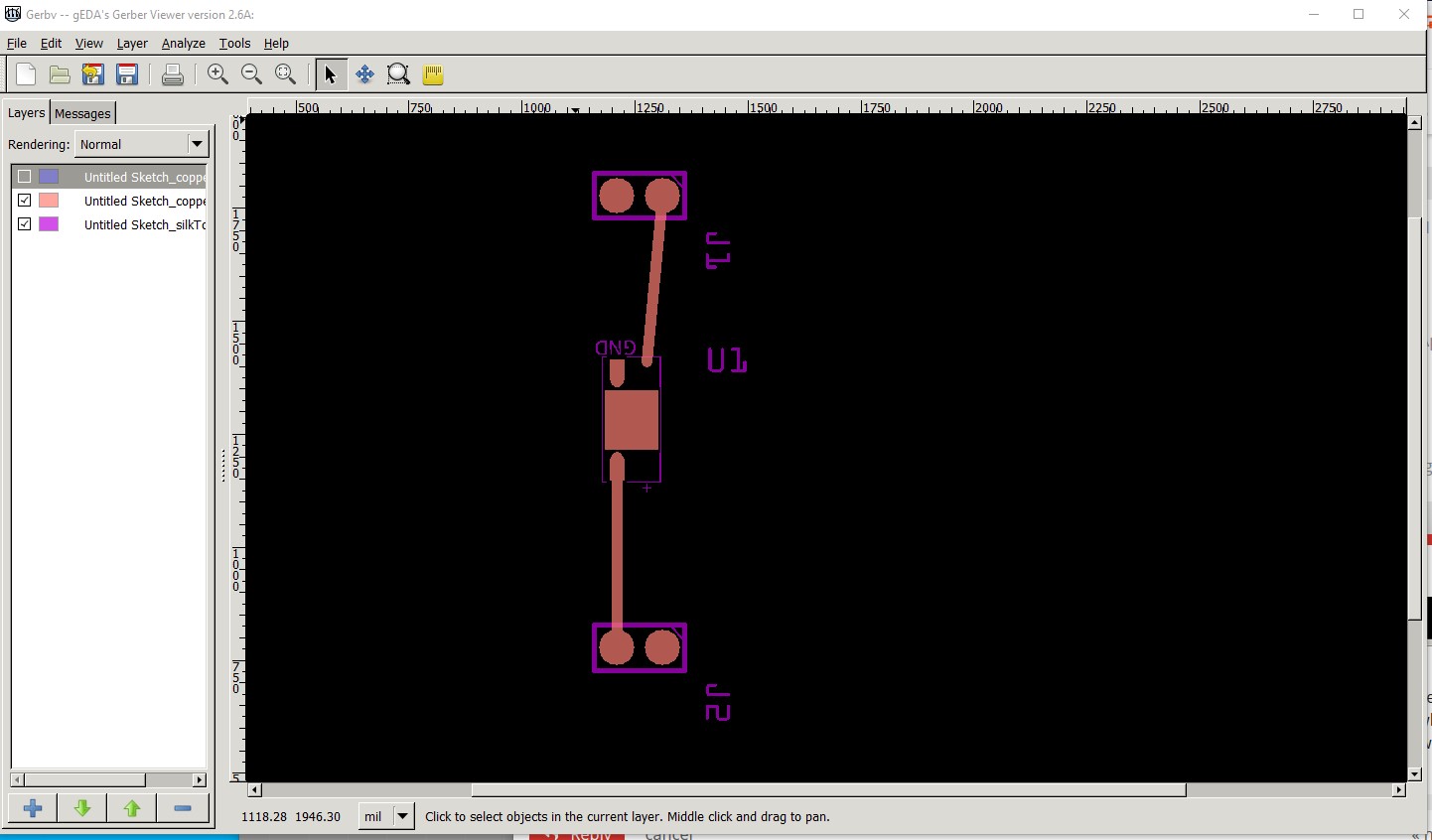
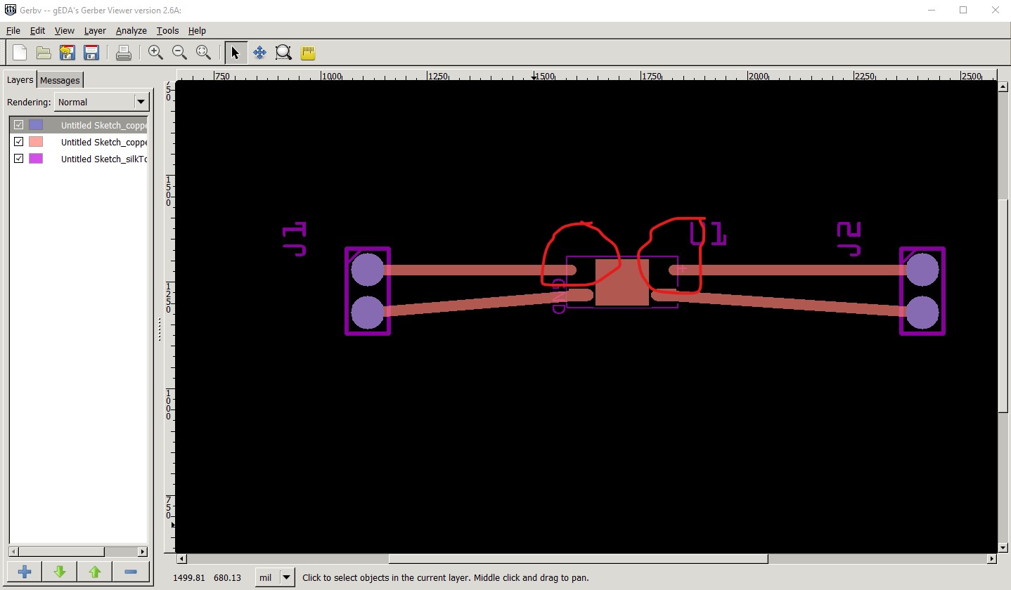
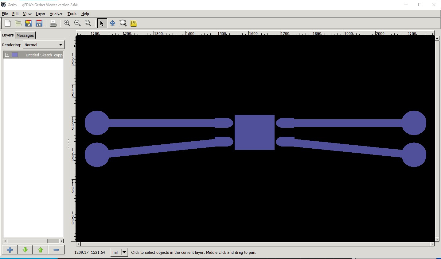
I then exported pcb as gerbers and looked at the gerber files in a gerber viewer (gerbv in this case) which shows some more problems (cause as yet undetermined.)
this is bottom layer, and we see the pads and the thermal pad (which we shouldn’t be) but not the two end pads (which we should be seeing!) It looks much the same when I switch to top copper layer:
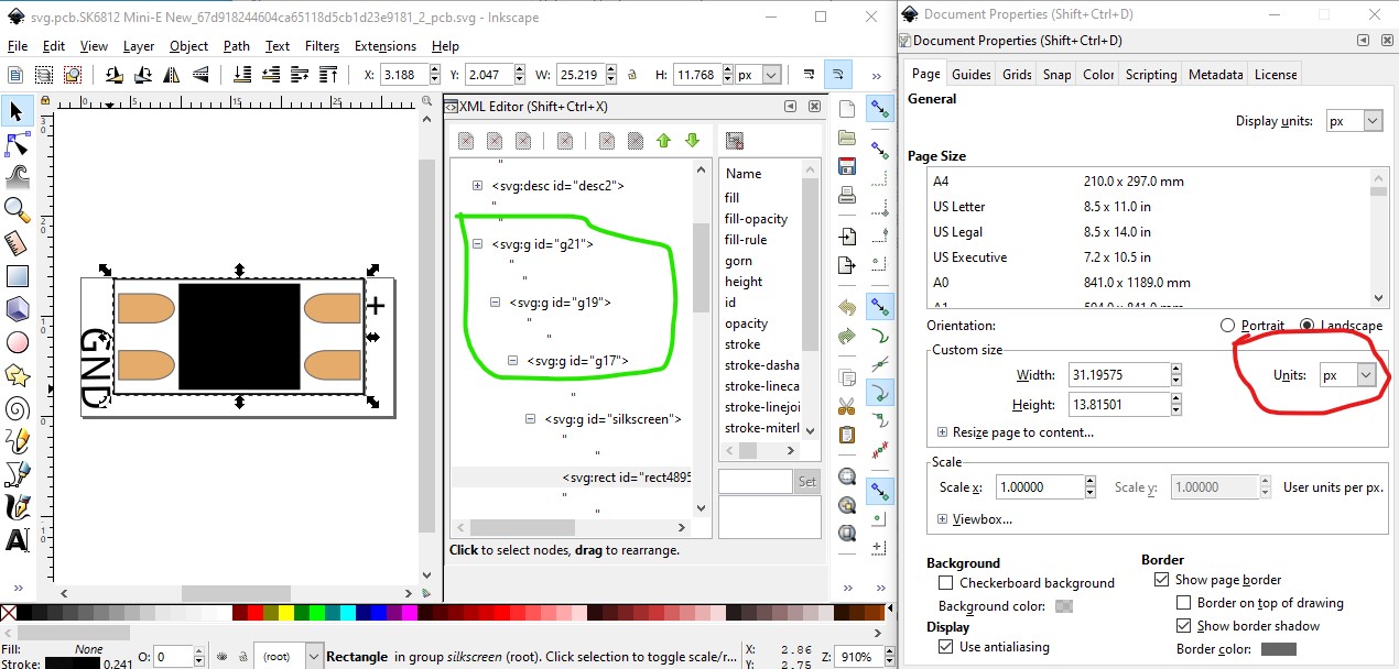
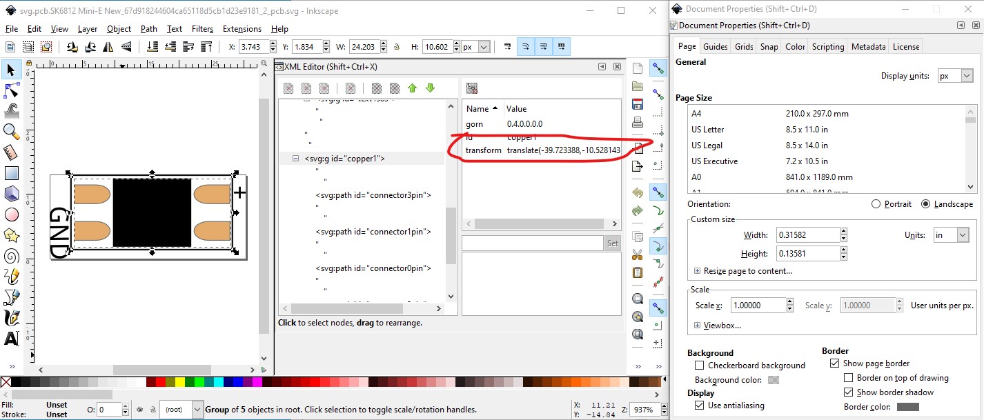
again the two end pads are missing. So now we need to go figure out why. So to start I edited the pcb svg in Inkscape
Several things wrong here. The Units (circled in red on the right) need to be set to in or mm. The image (which is selected by Edit->Select all) doesn’t start at 0 0 (cirlced in red at the top) so we need to do a Edit->Resize drawing to selection to correct that (and the viewbox at the same time.) This may be what is causing the pads to not be rendered. At the same time I am going to ungroup the uneeded groups above silk screen to reduce the clutter.
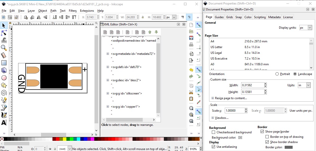
Here the groups have been simplified (I left the tspan group in place because an Inkscape bug changes the font size and it isn’t relevant at the moment.) Note the drawing (and the view box) now origin at 0 0 as it should. Next I am going to ungroup copper0 to delete it. Leaving only silkscreen and copper1 which is the correct configuration for an SMD part.
Now I save the file as plain svg and move on to schematic.
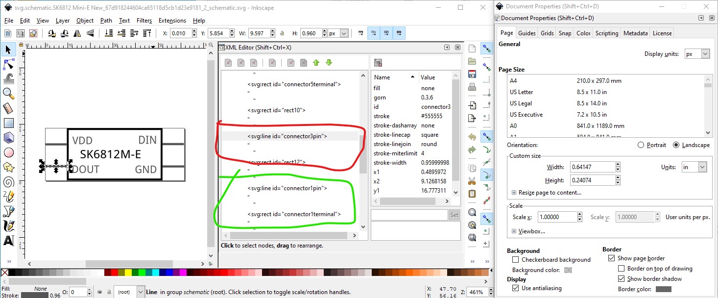
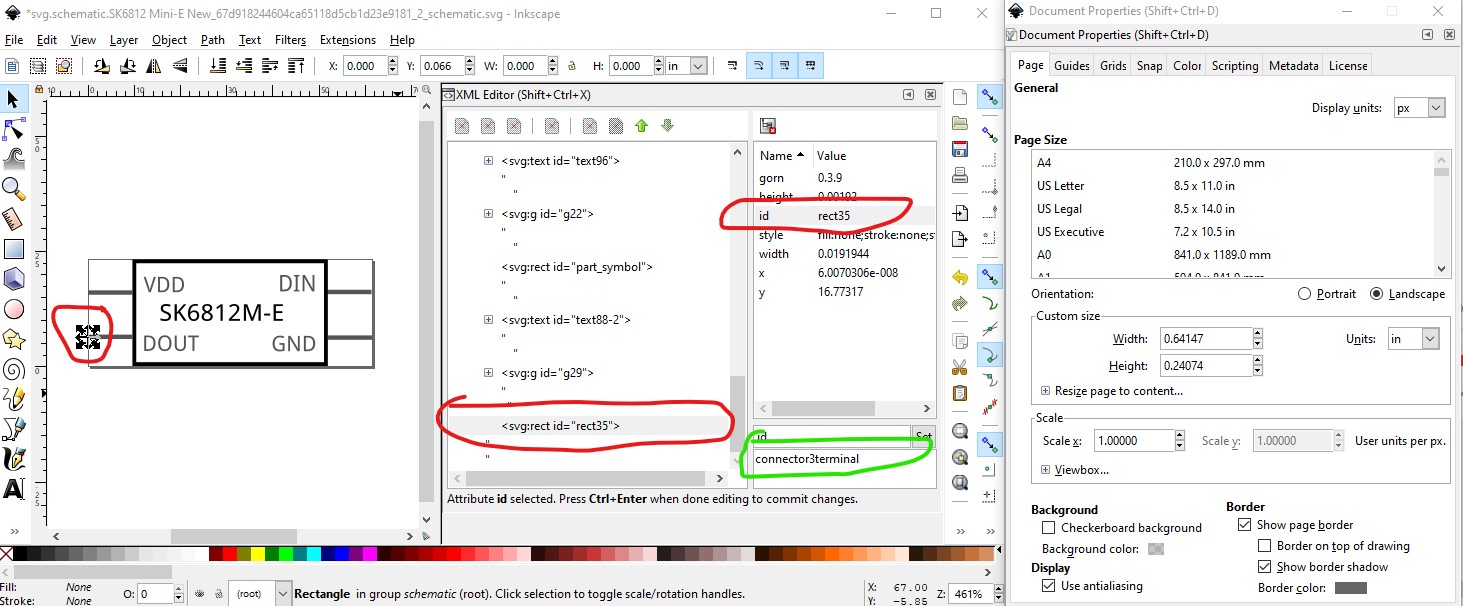
Schematic has Units in inches correctly already. But connector3pin lacks a corresponding connector3terminal (circled in red), connector1pin below it has a connector1terminal (circled in green) so I duplicated connector1terminal, renamed it connector3terminal and moved it down .1in to be on the end of connector3pin as it should be.
Then correct connector2pin (whose terminal is set as connector5terminal)
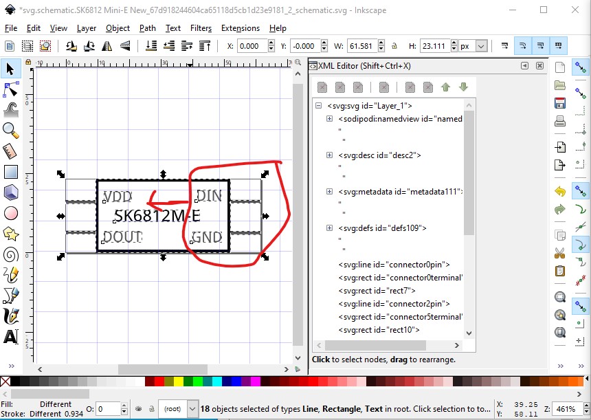
We see connector3 is now correct, so do the same to connector 0 whose terminal is named connector6. Then turn on the page grid (the grid is set to .1in on major lines, .01in on minor lines) and we see that schematic was mis aligned because the right hand pins are beyond the .1 in grid line.
and thus need to move a bit to the left to align exactly to the grid.
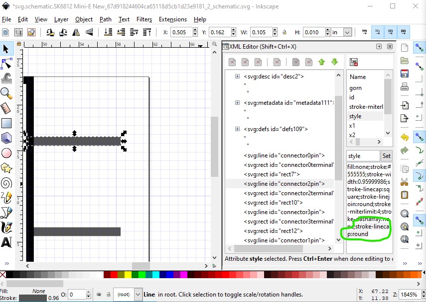
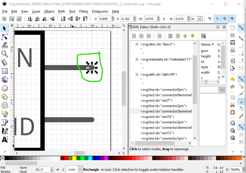
While I’m here I added a stroke-linecap:round to make the end of the lines round instead of square and changed the size and position of the terminal rectangle so it fits exactly on the .1in boundary and in the middle of the circular end cap on the line.
Then regrouped the entire image and set schematic as the group name and saved the file as plain svg. Now on to the fzp file to make sure all is well there. We need to remove copper0 from the entire .fzp file, starting with the layer definition:
<pcbView>
  <layers image="pcb/SK6812 Mini-E New_67d918244604ca65118d5cb1d23e9181_2_pcb.svg">
    <layer layerId="silkscreen"/>
    <layer layerId="copper1"/>
    <layer layerId="copper0"/>
  </layers>
</pcbView>
becomes
<pcbView>
  <layers image="pcb/SK6812 Mini-E New_67d918244604ca65118d5cb1d23e9181_2_pcb.svg">
    <layer layerId="silkscreen"/>
    <layer layerId="copper1"/>
  </layers>
</pcbView>
Then each connector definition needs copper0 removed
<pcbView>
      <p layer="copper1" svgId="connector0pin"/>
      <p layer="copper0" svgId="connector0pin"/>
    </pcbView>
becomes
<pcbView>
      <p layer="copper1" svgId="connector0pin"/>
    </pcbView>
  </views>
Now run the svgs through FritzingCheckPart.py to clean up and check for errors. Rezipped it to a new part and test
Schematic is now fine. The lines terminate correctly at the end of the pins, and the pins align to the .1in grid. Now on to pcb.
and pcb looks ok. It will only connect on the top layer (as the part is SMD.) Now to see if the gerber is happier.
No, still missing two of the pads. So back to the pcb svg to see why.
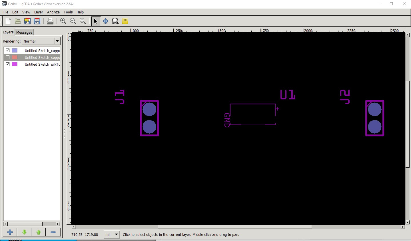
However copper bottom now shows no sign of the pads as it should
Well copper1 has a transform so lets start by trying to remove that.
to do so ungroup the entire svg (which usually removes transforms) and see what happens. It did indeed remove the transform, so lets see if that fixed the part. No cigar, still broken. That leaves us with something wrong about the path for the top two pads. So try duplicating and moving the bottom pads. Ungroup again because copying with groups will cause transforms. And success. There is something wrong either in Fritzing gerber processing (because pcb view is rendering the pads correctly) or the two paths. Duplicating and moving the bottom two pads to replace the top two pads makes things work.
We now have the missing pads in the gerber output. Here is the part that generated the above.
SK6812 Mini-E RGB LED-fixed.fzpz (12.0 KB)
Note you need to check the pads on pcb in this part to make sure they are the correct size because I changed px to in in Inkscape and the scale may be wrong depending on what dpi the original svg was in.
edit: Try this part with the ground fill and see if that cures the issue. If it doesn’t you may have hit a 0.9.6 bug as I remember someone else reporting a ground fill issue in 0.9.6 lately.
Peter