Clicking on the 10 of 11 nets routed (which should be routing complete) should show the unrouted net in yellow.
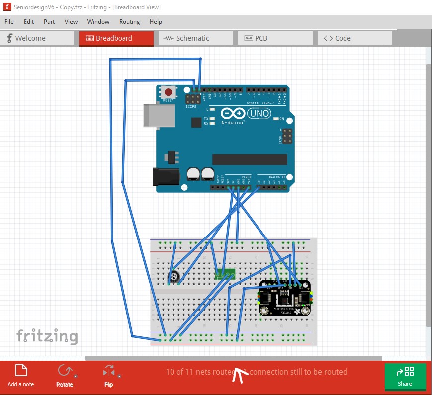
but instead shows this (which is wrong, indicating there is an error in one of the other views)

so change to schematic and delete all traces.
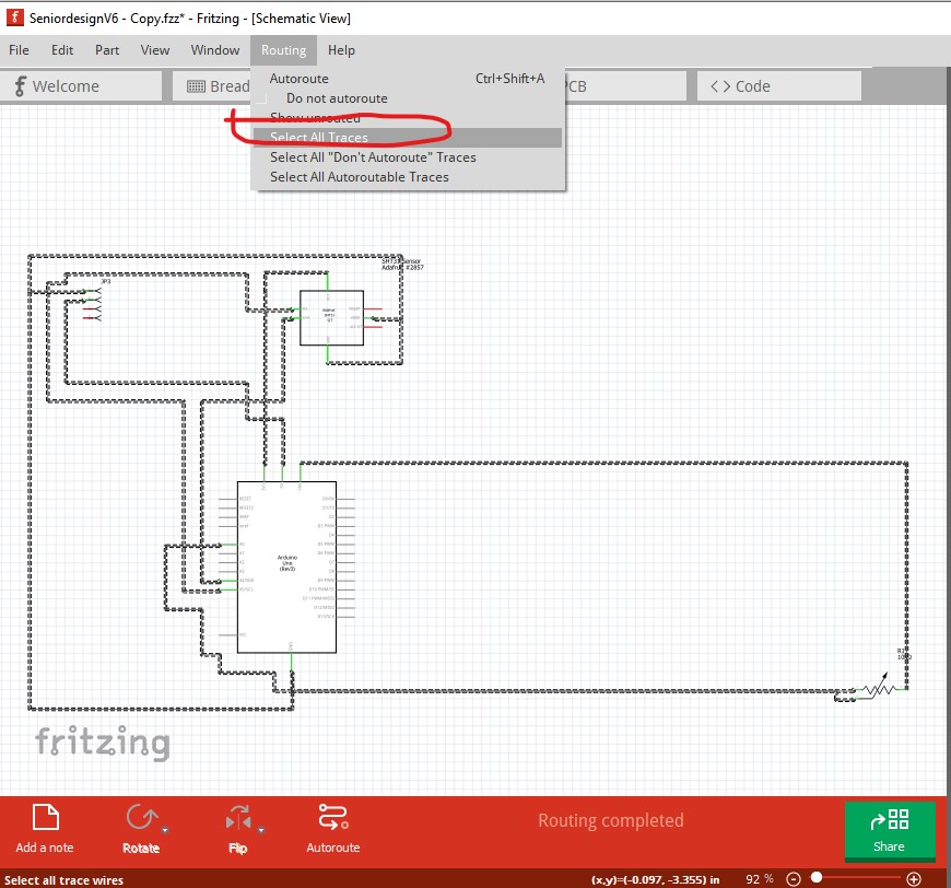
then hit the delete key to delete all the traces.
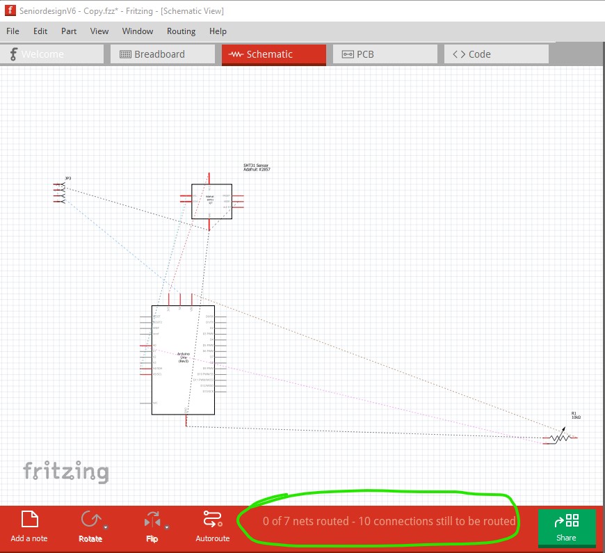
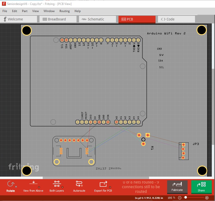
at this point it shows 0 of 7 known networks routed as it should (the 7 networks may be wrong as we haven’t deleted pcb yet though!) So change to pcb and do the same thing. Note it currently says routing completed at the bottom of the screen.

now hit the delete key to delete all traces.
Now we get 0 of 7 nets routed as we should and breadboard shows routing complete (so there was a conflict in one of the other views.)
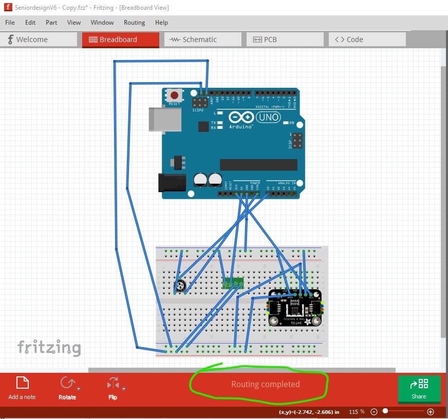
While it shows routing complete (because all the nets it thinks are connected are routed!) that is still not correct. There are 3 connections missing.
here the SDA net is missing the connection to the 4 pin header (the wires appear connected but don’t light yellow indicating a valid connection!) Same with the SCL connection, it doesn’t connect to the 4 pin header (and thus won’t show up in schematic or pcb as a connection.)
And finally the ground connection to the pot is also missing.
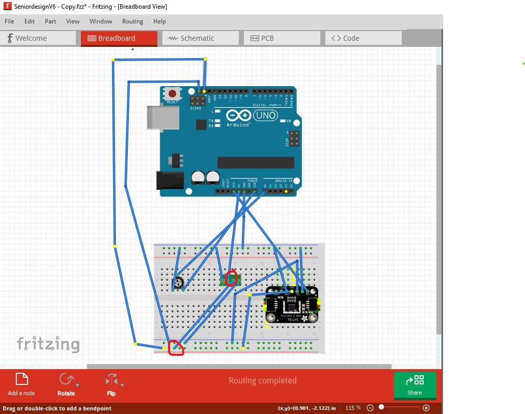
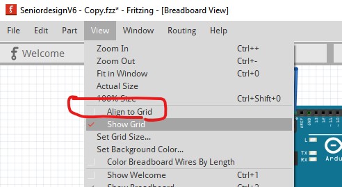
So first we need to fix all these problems. So start with enabling Align to grid (which is on by default, so you must have disabled it at some point, which is a bad thing to do in breadboard!)
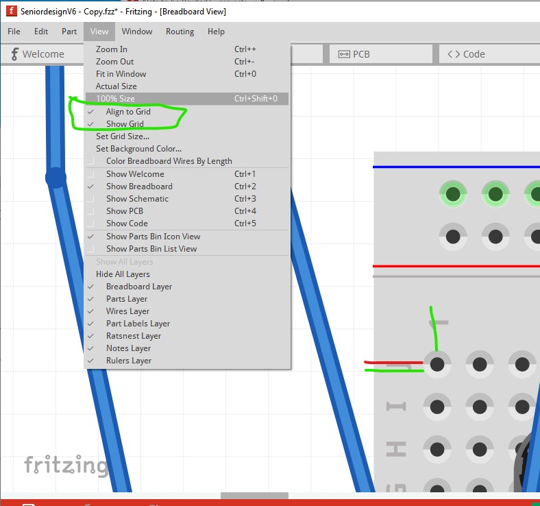
so set align to grid (which won’t take effect until we move all the parts!)
Note the breadboard holes do not currently align to the grid. They are slightly offset in y from the grid (the red line is the center of the pin the green is the grid.) Clicking on the breadboard and moving it slightly in x and y will cause it to snap to the grid.

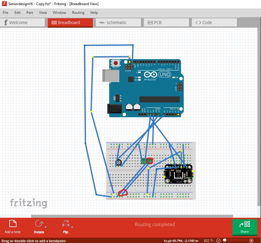
Now move the pot a couple of positions along in X. Note that its 3 connections to the breadboard are green indicating they have connected to the breadboard as are the three wires that were going to the pot.

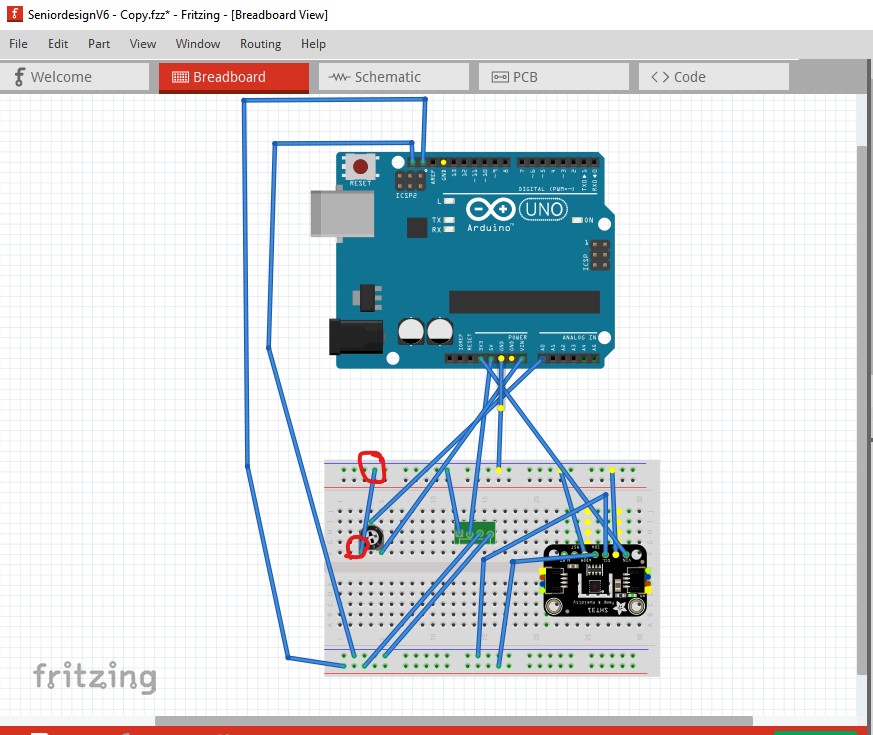
now move the pot back to the wires (note I also moved the wires so they connect to the breadboard as they have to in real life rather than the pins on the part!) I also changed the color and positioning of the wires to make the connections clearer and as short as possible. Now when I click on any ground pin all the grounds light up yellow:

As do all the other pins. I’ll note in passing, that the pot connecting to Vin (typically 6 to 9V) with the wiper going to the A0 pin is dangerous because the A0 pin is limited to 5V in (and thus the top of the pot should more likely connect to 5V!) As well you need a level translator from 5V to 3.3V (such as this adafruit device
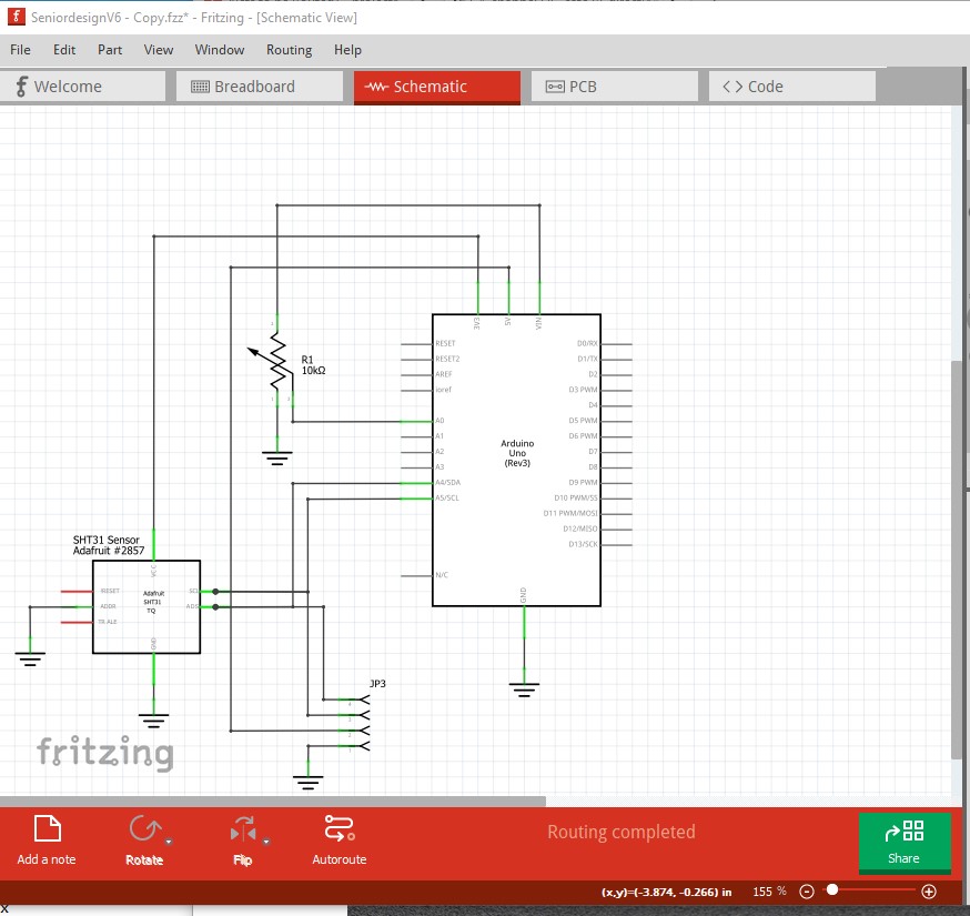
on the SCL and SDA lines to protect the 3.3V inputs of the SHT31 sensor or change to a 3.3V Nano instead of the current 5V Uno. At this point breadboard appears to be correct and routing is complete so now we move on to schematic. First move the components around until the routing looks correct, then click on the rats nest lines one at a time (to route them) then move the wires in to a sensible position until routing is complete:
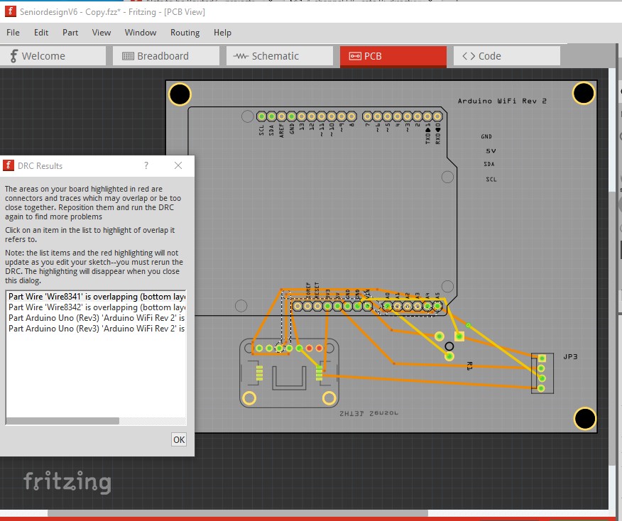
then move on to pcb and autoroute it. As usual autoroute does a poor job (it doesn’t pass DRC for instance)
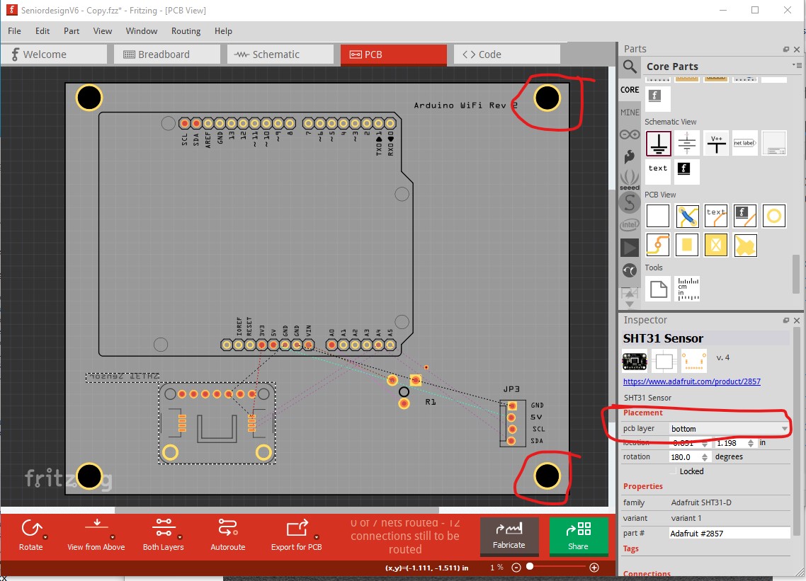
For some reason the SH31 is on the bottom of the pcb rather than the top. I assumed this is an error and moved it to the top of the pcb. The holes for the mounts are outside the pcb area (and will thus be truncated and are thus likely incorrect and need to be moved) The labels for the header were in the wrong place.
When I autoroute that it works and passes DRC, but is likely not optimal as it is making connections to the SMD pads which are likely not accessable on the part (as they appear to be SMD connectors.)
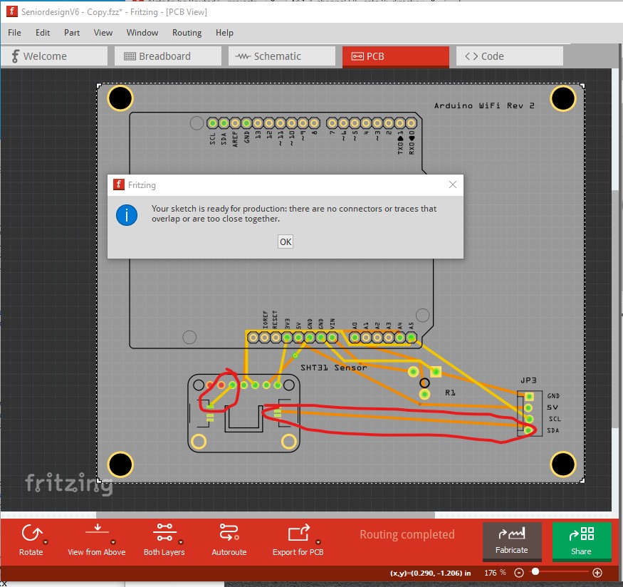
So delete all the traces and manually route the board. Which procduces this which likely will do what you need.

which comes from this sketch
SeniordesignV6 - Copy-fixed.fzz (36.9 KB)
Peter