Temporarily moving J16 outside of the PCB boundary will prevent auto route from making any connections to it. However, that will also not “reserve” the space where J16 is supposed to be, and autoroute uses it for some of the traces. To handle that, create a duplicate of J16, that does not have any connections to it, and position it where J16 is supposed to be. Then autoroute does what I think you want. Finish up by remove the duplicate, and moving J16 back onto the pcb.
Autoroute does not do a very good job for some things. After running autoroute, run Design Rules check. There are a lot of things then need to be cleaned up, because autoroute cut a little too close to the connector pads. There are also a lot of the generated traces that can be cleaned up, straightened, simplified.
Thanks for your help.
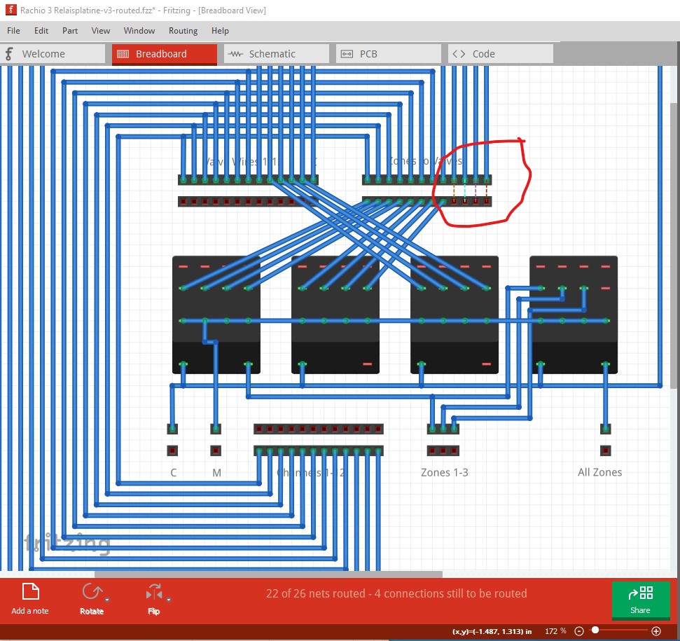
When I move the J16 outside the PCB boundary, I also lose all connections from J4 to J16 and therefore are not able any more to stick jumper wires between these two pin headers to route a channel/valve to a specific relay.
The pin headers in breadboard view that don’t have any connections are only placeholders for the later WAGO Terminal Strip with 2 solder pins I will use.
You look to have run in to a Fritizng bug. We think (because we have not been able to reproduce it) that it is caused by making an incorrect change in another view in some sequence which causes corruption in the routing data base. To fix this I deleted all traces in all views (which appears to reset the data base, although it did not the first time I tried this.) As well I made some changes in pcb view
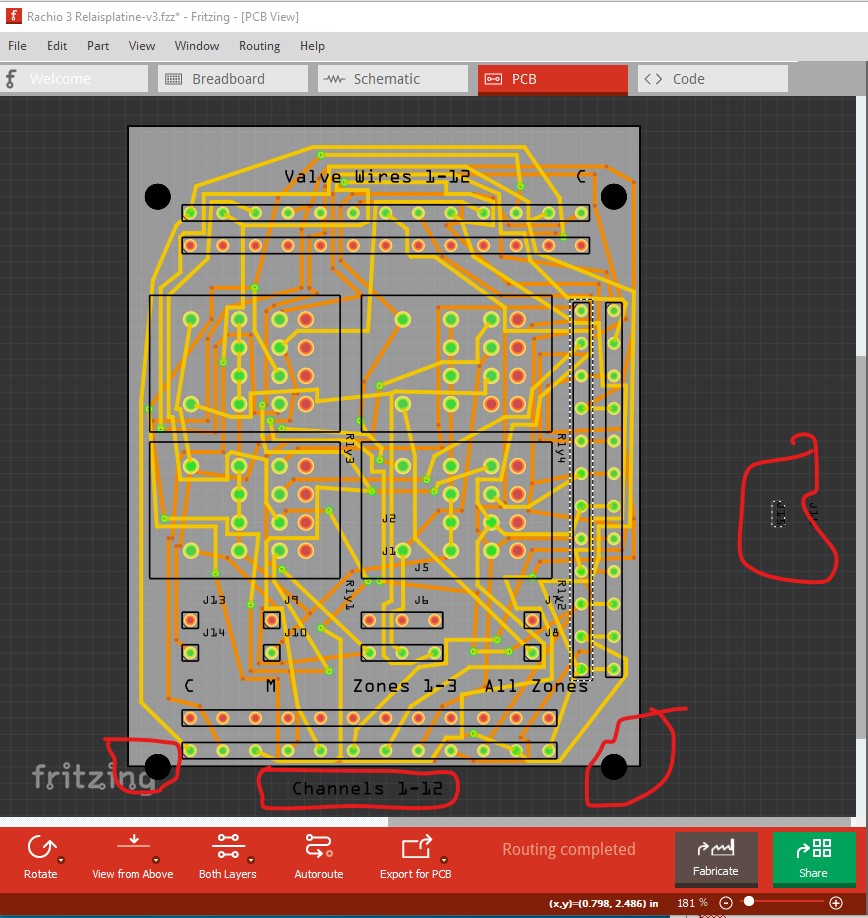
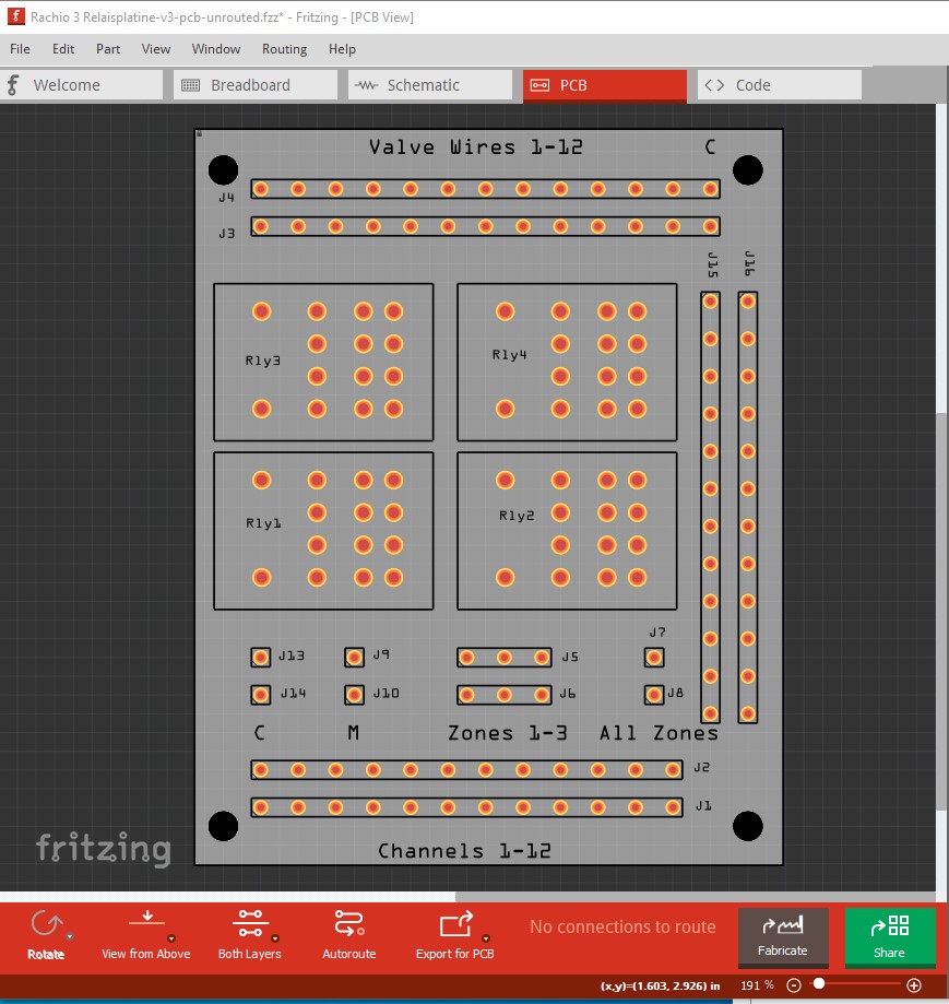
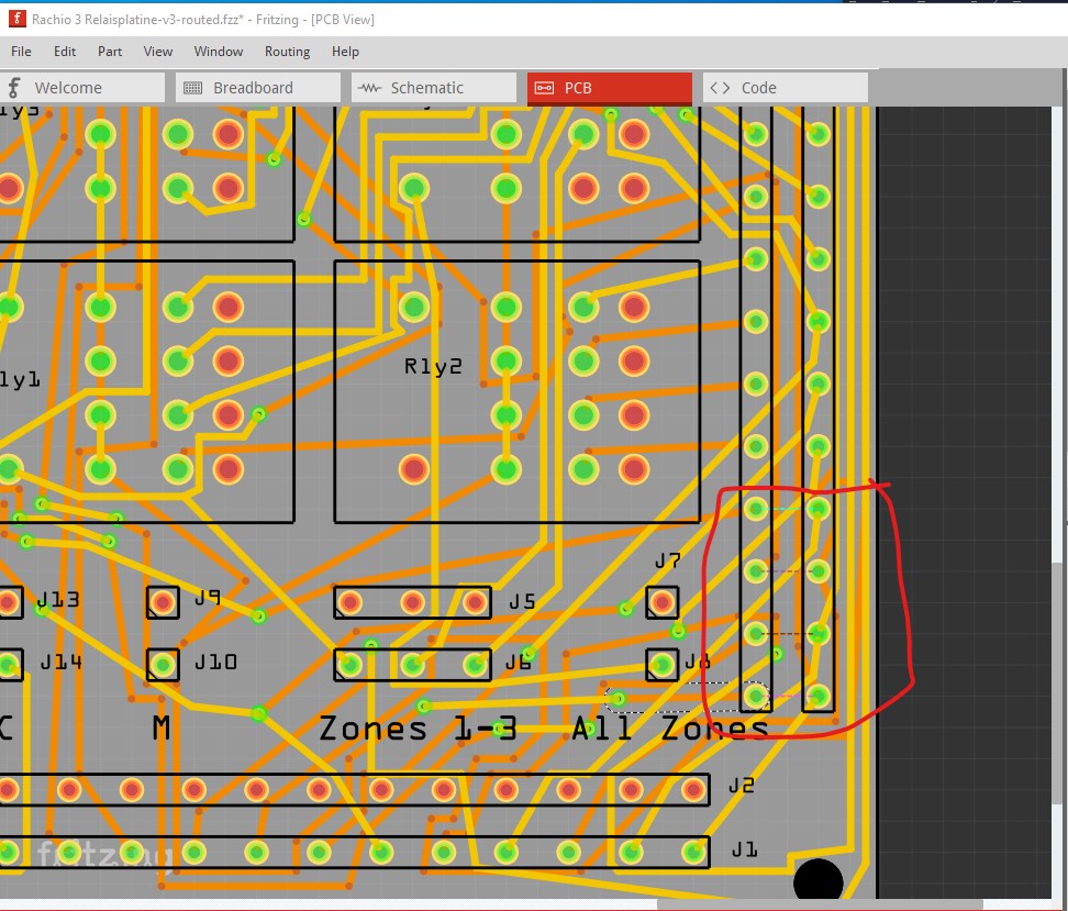
the pcb outline is a little high. The mounting holes and the channel label are off the board and won’t show in the gerber output. As well a number of the part labels are off the board. I moved things around to correct those and deleted all traces in all views to produce this
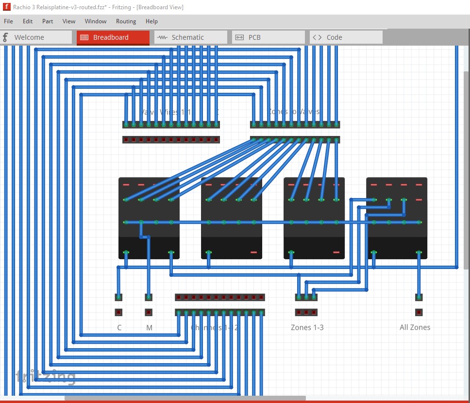
As noted all traces and vias in all three views have been removed to clear the routing database. Now you need to re do the wires in breadboard. Then using autoroute in pcb should route pcb correctly and you can then route schematic by clicking on each rats nest line and dragging it to an appropriate position. We recommend making the complete circuit in one view, then moving on to the other views and routing them via the rats nest line to avoid this problem. At some point (although it has been about 5 years that I have been trying without success) I hope to be able to recreate this problem because then we could find and fix it. All the cases I have are after the damage has been done, and even trying the things I think the user did to create the current sketch have never caused the problem. There is either something I am missing, or some step that has been deleted in all the examples I have seen.
Here is a copy of the sketch with all the traces removed
When I did my test, the ratsnest lines remained between J4 and J16. I think there were only 2. So, after putting J16 back on the PCB, those 2 traces would need to be routed manually. Another more complex trick (I have not tested this), would be to connect ONLY the J4 wires to that temporary duplicate of J16 (using breadboard view). Then autoroute should handle those wires on PCB view. To cleanup, use “Delete minus” on the temporary duplicate, move the real J16 back where it belongs, and move/drag the ends of the traces from J14 so that they actually attach (instead of just looking attached) to the J16 connector pads. This process will need cleanup on the breadboard view as well, to get rid of the dangling wires that were hooked to the duplicate of J16.
EDIT:
Above is not going to work.
After a closer look at breadboard view, deleting all traces from PCB view, and checking some connections on both PCB and breadboard view, I agree with Peter. The ratsnest wires on PCB view do not match the wires on breadboard view. Deleting all traces on pcb (routing menu, select all traces, delete), then doing the same on breadboard view (select all wires), followed by re-adding the wires in breadboard view, and finally autorouting pcb MAY work.
I do not know if autrouting will work after than. The problem is that EVERY single pin of J16 connects to a pin of J4, so 12 paths need to be found from J4 to J16, while still having room to connect the 12 J15 pins where they belong. There does not seem to be enough physical space on the pcb do do that. At least with a 2 layer board, which is all the Fritzing can handle. Maybe if you change the traces width to a very small size. Which is not a good idea when they need to carry power, not just digital signals.
EDIT2: I see that some of the common (grounds?) are connected in schematic view. Delete those along with the rest.
Yes that is possible! I changed the views sometimes for better overview.
Upps… didn’t even realize that, but you are right! argh
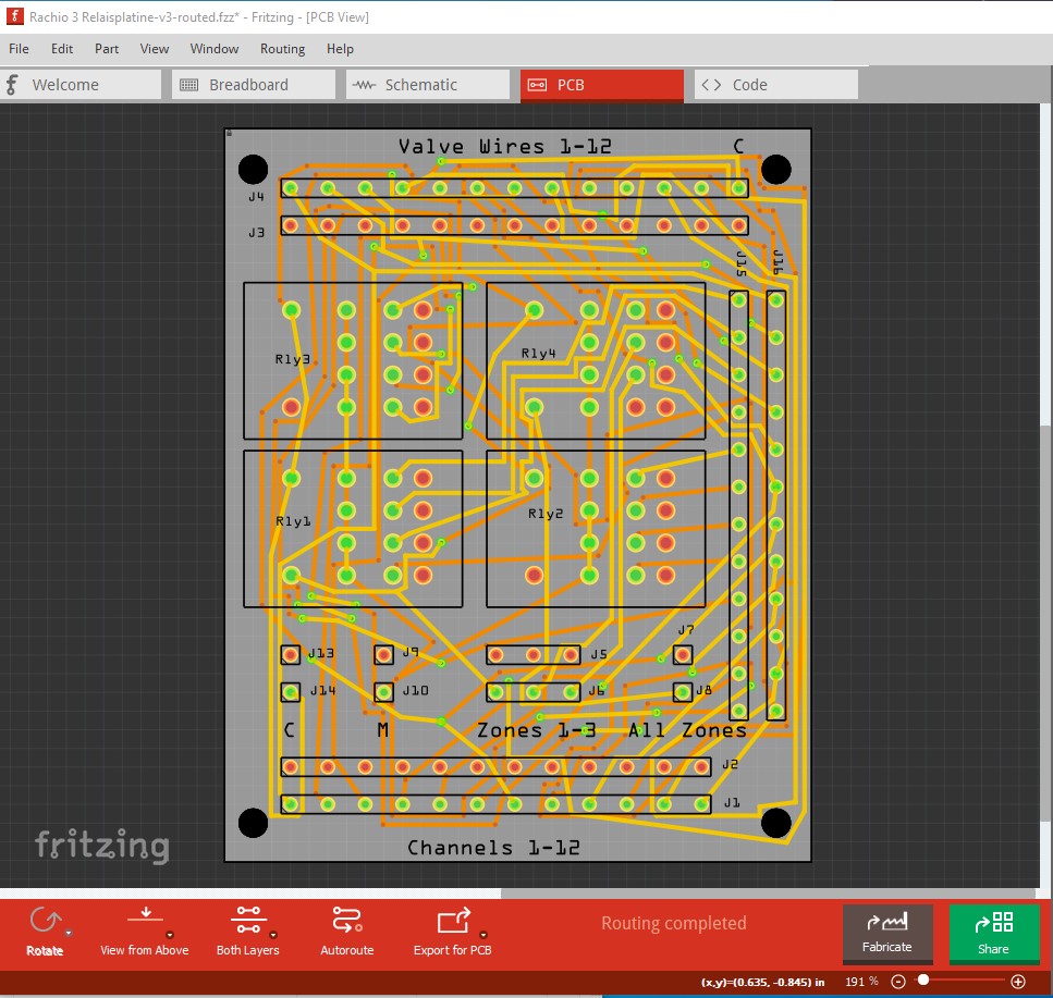
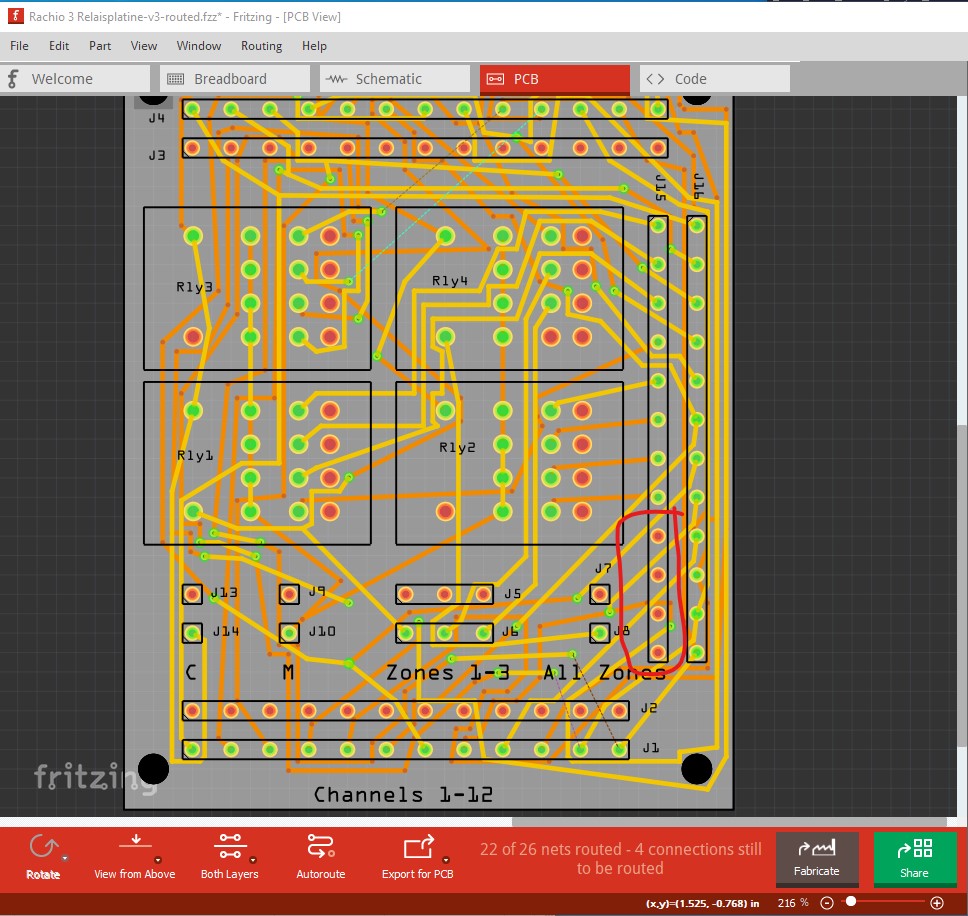
Awesome! It works now! I had to make the PCB a little bit larger for autoroute to connect all connectors. EDIT: Increased autorouting results from 100 to 1000 and got a result even with my 80x100mm PCB!
I will do so in the future, I swear!
I think I won’t be able to help find the error, as I’ve been sitting on the board project on and off for a few minutes per weeek /month since early 2020, and since then a few updates to the software have also appeared, which of course I’ve always updated.
You saved my day! Many thanks!
No need to do this again as re-routing the connections with your unrouted template works perfectly fine!
I attached the final PCB for others who want to combine Rachio irrigantion channels to fewer zones.
That has been the general case in the past too. You make changes and don’t notice things have gone wrong until it is too late. I hope one day to stumble across a way to reproduce this, but so far no luck.
Maybe I have an idea how to recreate the bug. As far as I know I deleted several connections, recreated connections and as you can see in my first PCB layout there are these dotted connections lines in breadboard view which I cound’t get rid off.
Yes, that is the general description of the path that causes the problem. However, there is another factor. Deliberately doing that has not been able to recreate the problem in testing. There is something else in the sequence that is needed to trigger the connection database corruption.
We see rats nest lines for the new connections in breadboard. However if I delete the wires in pcb, the rats nest lines in breadboard disappear as they should.
Maybe the problem only exists in the macos version?
Or the problem is already solved, since I started using Fritzing with version 0.9.3b
Anyways… thanks a lot for the immediate help that solved my problem! The PCB is already ordered.
No, it is in all version and all operating systems (I first ran in to it on 0.9.3b and it is still here on 0.9.6) As long as we fixed your problem, all is well. Hopefully eventually we will find a way to recreate the problem so we can fix it.