Can anyone point me to the foot print of Heltec CubeCell HTCC-AM01module?
There doesn’t appear to be a part and there isn’t enough information available to make one. We would need a recommended pcb footprint document to make a footprint and I don’t see one.
Peter
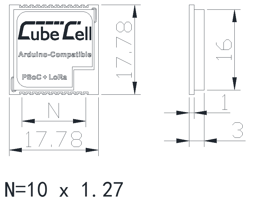
Sorry, to reply lately. I cannot find more details drawing on Internet too. Contacted manufacturing also does not get any helpful information. Only got an https://resource.heltec.cn/download/CubeCell/HTCC-AM01_Module/sch_pcb_package.zip for other PCB Design program. Will it be possible to convert this lib into Fritzing format.
Somsak
Unfortunately doesn’t look helpful. They are in PcbLib and SchLib format and I don’t know which EDA package that is (and I likely won’t have it anyway.) There is an EasyEDA footprint available but again it appears as an image without any dimensions. I’ll poke at that again and see if I can figure something out.
Edit: So when the going gets tough, the tough resort to png files. I imported the above png file and used it to make a part. The pads should be fine (if a little tightly spaced) as the pitch if not the pad size is documented. There is only about 10thou clearance between pads, but I am told the cheap board houses will take down to about 8thou spacing, but you may need to check with the people you use. Tell us if it works  .
.
HelTec-HTCC-AM01.fzpz (5.9 KB)
Peter
Thank you. I will try it and hopefully it will work on the first time.
Somsak
Print the pcb footprint out at 1:1 scale (probably on a transparant page) and compare it to a real part before ordering boards. While it should be fine, better safe than sorry!
Peter
1 Like