how can i do this? i tried dragging a rectangle around them but then when i drag the selected items, it only moves the one i clicked on to start the drag.
No, as far as I know you have to manually move the bend points unfortunately. There likely isn’t any way for the program to know where the bends should move to.
Not that big a kink. You can select the bend points or the wire and reroute the trace, which you probably need to do anyway to make the routing work given there are likely to be other traces in the way of the move.
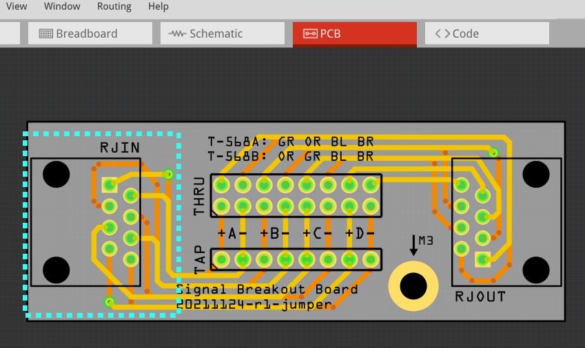
i guess but… well i mean in my case that blue dotted section just needs to move about 0.2" to the right. there’s clearance for it (that’s why i want to move it). need to move the group on the right about 0.5" to the left too (dropping that screw hole of course).
it’s about a 20 minute tedious job; whereas if i could select and move it’d take just a second and also give an opportunity to do things like “oh 0.2 to the right is a bit much let’s see what 0.15 looks like” or “now that i think about it, i want that screw hole back”. it’s totally doable though; but it’s an annoying time sink.
i dunno; it’s on the top of my wish list. to me, anyways, it seems like it’d be a basic feature. i’m not sure if i can think of any other software that involves graphically connecting nodes with pathed edges, where you can’t move a selection of the edge’s path points along with everything else.
anyways it is what it is i’ve gotta close the browser now and mentally prepare to move 34 closely spaced bend points a few pixels to the right, heh… and then i need to move the similarily complex portion on the right side of the board a little to the left, too. then i might need to look around for a uh … “trial version” of eagle or something, heh.
There is a free version of Eagle (limited in board size I think) however it is much more complex to use than Fritzing. There is also Kicad which is also open source. I don’t know if either of them do this though.
i was able to figure out a kludgy workaround, although i’m not sure if it is more or less tedious. basically:
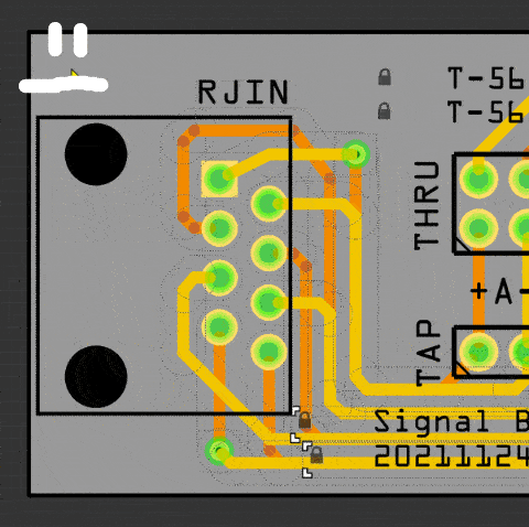
remove any wire segments that cross the boundary of the selection area: you can create strategic bendpoints if necessary then right-click the wire sections and “delete wire up to bendpoints” to remove the segment.
do not move the pcb out of the way: select the group of parts and wires that you want to move but also make sure the pcb itself is part of the selection! for some reason, bend points of selected wires are not moved if the pcb is not under them.
now drag the whole group somewhere to move it.
put the pcb back where it’s supposed to be.
reconnect the wire segments that were removed in step 1.
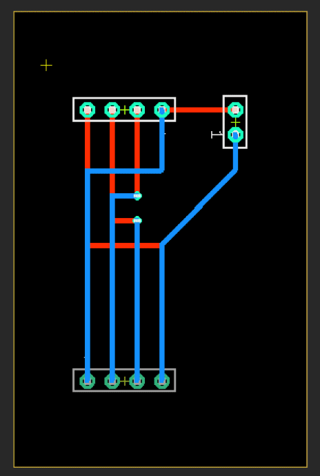
here’s an example:
now, there’s still a bunch of issues that make this “workaround” a bit of a pain in itself:
you’ll have to select a lot of things, which is always a battle when elements are close together.
afaik for some reason you can’t connect wires directly between two bend points: you have to move one bend point to another one. this means that you might have to recreate and reposition any bend points you lost here. depending on how you did step 1, you’ll either have created those temporary bend points or you’ll have to replace merged points, which means either way, you can’t avoid having to click the mouse at least once per wire that crosses the selection boundary.
you’re also still going to have to click and reposition one bend point per wire after reconnecting the wires anyways. this is because fritzing seems to have some weird bug where when you connect a wire to a bend point, the destination bend point ends up in the position you released the mouse button and ignores the grid snap settings. so you’ll have to nudge it back to its original position after reconnecting the wires. this, as usual, runs the risk of driving you insane if your wires are close together, trying to convince fritzing to select the correct element.
you’ve got to move your pcb. so if it’s sticky and you don’t want to reposition parts that are stuck to it, you’ll have to temporarily unsticky it. also you’ll have to move it back to where it belongs.
it’s pretty easy to select parts and the pcb when the parts are on the edge of the pcb. however, if your parts are in the middle of your pcb it could get a little trickier.
so yeah, you kind of have to judge if temporarily removing wire sections is going to save you time and brain cells compared to moving all the bend points individually, but, it’s an option.
it’s still a lot of work for something that seems like it should be straightforward (i.e. moving stuff) but, i dunno. it helped in my case.
Minor variation on the @jasonc workaround.
To prevent needing to move the PCB back, before starting this, set the lock flag for the PCB. That way, even though it is (and needs to be?) selected, it will not move.
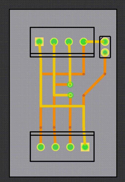
Another small speedup. When reconnecting the wires, instead of ‘nudging’ them back into position, double click the created bend/join point. That will delete the bend, which, for the example, will nicely clean the trace up.
There is a free version of Eagle (limited in board size I think) however it is much more complex to use than Fritzing. … I don’t know if either of them do this though.
^ eagle
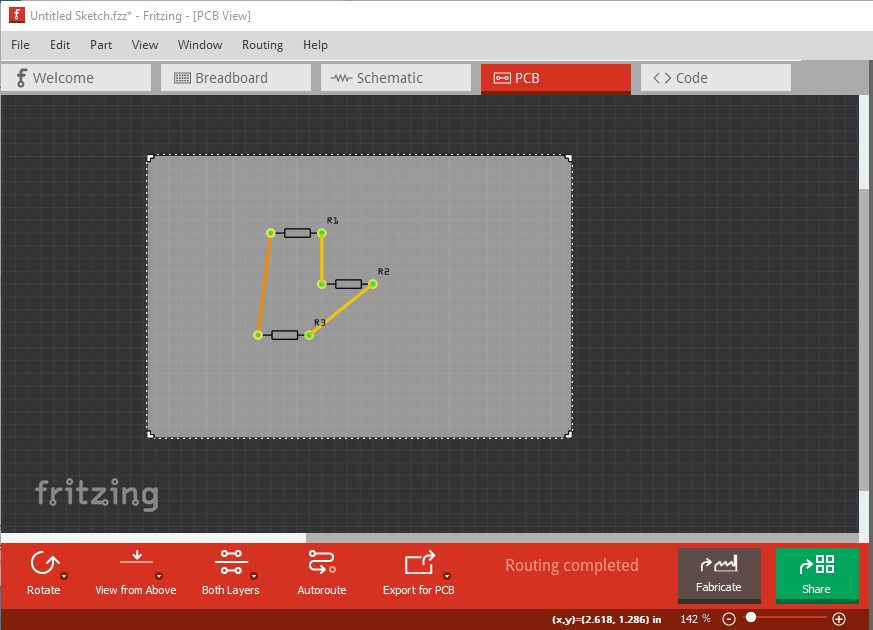
i’m not familiar with kicad but i think it also will automatically push other traces around to avoid conflicts in block moves, or so i hear.