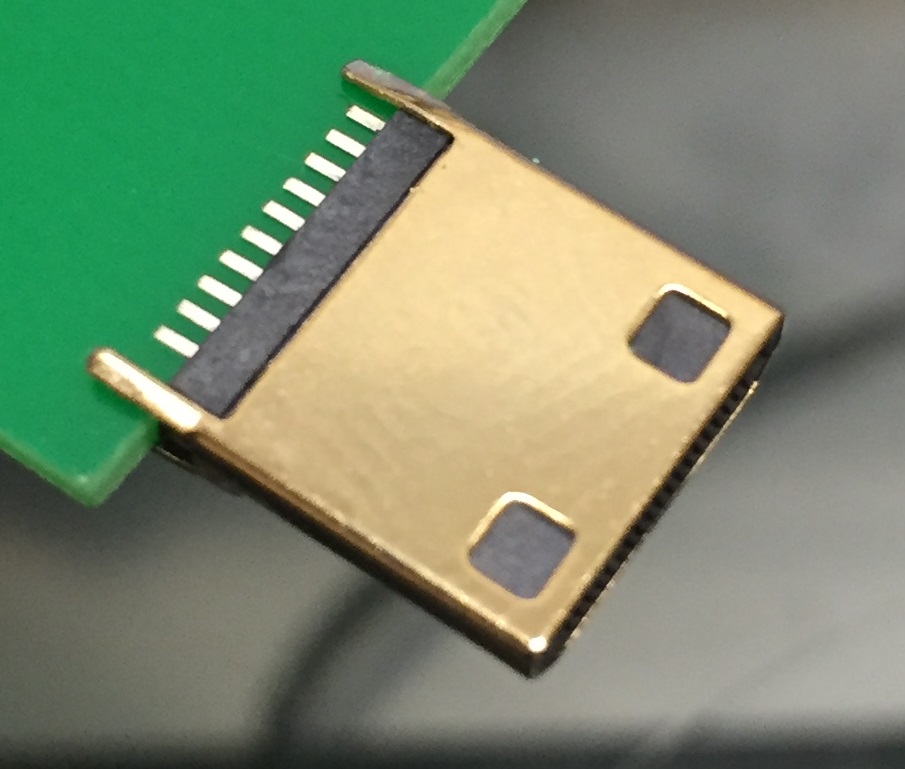
I have a mid-mount SMT component that I need to make for Fritzing. How do I create a part that has pads on both the top and bottom layers. Attached is a picture of the part in question.
If you know how to make parts you group the pads in copper0, and put that in another group called copper1.
I don’t think that will work here. I think he needs pads on both sides of the board that are independent (like an edge connector) and that is difficult to arrange. It think this thing needs 10 pads on top (connector0 -9) and 10 on the bottom (connector 10-19).
Peter
Correct. The part mounts on the side of the board and has pins on top and bottom. 10 on bottom and 9 on top or vise versa.
The last time we did this (an edge connector), I think we ended up with two parts, each smd one for the top and one for the bottom with alignment the responsibility of the user. I’ll poke at it in a while and see if I can figure something out, but we didn’t find a solution that worked last time.
edit:
Looks like it is possible with some limitations. The main one is you can’t flip the part to the bottom of the board which in this case should not be a show stopper (you can create the part on the bottom if you need that direction). You can’t do this in parts editor you need to edit the underlying files, how experienced are you at making parts (hint this isn;t a good first part)? This is the gerber output of a 8pin ic with half the pins on top and half on the bottom (in practice on an IC this won’t work, but for your part it will)
To do what you need you (or I) would need to move the pads on top over the ones on the bottom (which I was too lazy to do here.)
Peter
1 Like
Opps, now I remember.
So you have to make 1 part with only copper1 and another with only copper0, then just stack them on top of each other.
No, this one is a single part, with both copper0 and copper1, but not grouped together in the svg. The fzp has both layers but the pins only use on layer or the other (half in copper0 half in copper1). The problem is this was how all parts were in the past and Fritzing tries to deal with that which breaks the top/bottom of the board logic (and perhaps more I haven’t found yet), but it should work for that the OP wants to do I think.
edit: a part is worth a 1000 words 
dip8-smd.fzpz (5.9 KB)
Peter
I was thinking about separated copper groups in one part, because I used to see it a lot in the FZ 9.2 days. If I get the time I might make a part with stacked pads just to see how to make connections to top and bottom. 
Thanks! This will be a great place to start.
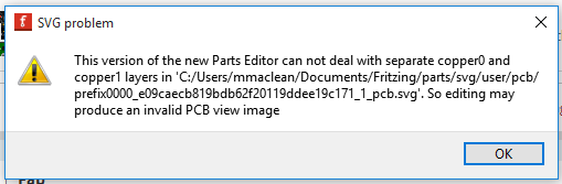
I am getting this error. Should I be concerned?
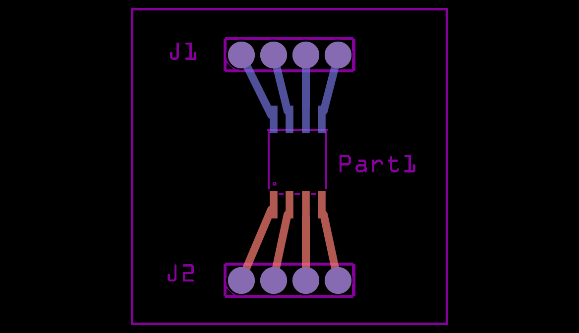
Can y’all look over this part to see if you can find anything glaringly wrong?MiniHDMI.fzpz (6.1 KB)
No, it is just telling you that it has what it thinks is an old part (instead of one that we have screwed with to do what we want). It can be ignored, although your part won’t correctly change to the bottom of the board due to this, you likely won’t care.
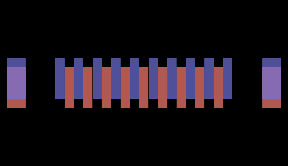
Your fatal problem is the fzp file is incorrect, you only have copper1 and thus only have pads on one side of the board. Secondary problems (but can be ignored) are incomplete schematic or breadboard views. In addition the pads from top to bottom are offset in y which may not be correct as this image from the gerbv geber viewer demonstrates (with a corrected fzp file). Purple is bottom layer orange is top layer
If you have the data sheet for the connector I can fix this up for you if you like. This part contains the corrected fzp file which generates the above gerber output (I was too lazy to make a new part so you will need to remove your current part and restart fritzing to load this)
MiniHDMI-fixed.fzpz (6.2 KB)
Peter
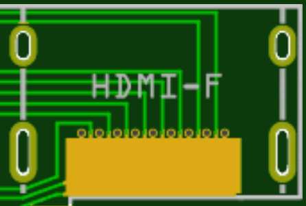
Is this what you are getting when you add the part?
Yes. The red is because you don’t have enough connectors in schematic or breadboard. It should work fine in pcb like this however.
edit: I spoke too soon, there is more wrong than just the missing connectors. I ended up having to complete schematic to identify all the problems. The internal pin numbering was wrong as well. It is corrected (all of it, the missing connectors have been added to breadboard although it is not complete and schematic as noted has been completed).
MiniHDMI-fixed.fzpz (8.2 KB)

Peter
I regret to say that it is not working correctly. When I add the part to my project the PCB view looks like this.

I can’t click on any of the connectors.
Here is the part that I have created. It worked great until I switched the copper layers and now there is the big red bar across it which prohibits me from connecting to the connectors.
Generic female header - 23 pins.fzpz (7.9 KB)
That is likely because you have transforms in the pcb svg. The gerber code is not all that xml aware and has a few issues (not processing inheritance and not processing transforms being two of them). To fix this I edited the pcb svg in Inkscape and changed the fill on the text from #ffffff to #000000 (from white to black so I can see it to make sure it doesn’t move as the translates are removed), then ungrouped everything under silkscreen to leave only the three paths and the 2 texts (no groups) as well as the group containing the group silkscreen. At this point silkscreen still has a transform though, so now select the group silkscreen and ungroup then immediately regroup it. That removes the translates on the ungroup and regroups silkscreen (without the transform this time). Now do the same to copper1 and copper0 (copper0 has a bunch of subgroups as well). If you look at copper1 and copper0 in the xml editor you will discover they have non identical transforms which breaks gerber processing. Again select copper1 ungroup it and regroup it to remove the transform and re establish the correct grouping. Then save it as plain svg (I’m assuming Inkscape here!). However that doesn’t fix the problem, the connectors are still unhappy in Fritzing. It looks like you have generated a new part using the parts editor and not edited the fzp file. At present the fzp file has both copper0 and copper1 specified for each connector, in this configuration the connector needs to have only copper0 or copper1 (depending on which layer it is on) so you need to hand edit the fzp file with a text editor to make that occur. Since copper0 is odd numbered pins and copper1 is even, you need to remove the copper1 layer in the pcbView for the odd numbered pins and the copper0 layer for the even numbered pins. Except for connector19 (in copper1 not copper0) and connector22 which is in copper0 rather than copper1 (I would probably reverse those two to be less confusing ). That still doesn’t fix the problem though. A trip through that parts check script flagged translates in pcb. A check indicates the pins have a scale (-1,0) translate (usually from rotating the pins). Removed them manually by copying the x coord in the tool bar, deleting the translate, then resetting the saved x coord in the tool bar. That didn’t fix it either (and may not be a problem). So in the fzp file change the family from “Pin Header” (which likely trips off special handling code) to "hdmi connector"from my original part. That didn’t help either. Move back to my original hdmi connector part and substitute your pcb file in to it. Discover my problem is I had some of the last 5 pins swapped between copper1 and copper0, correcting that fixes the part. Now to see how few of the changes above are actually needed. In order for top or bottom of the board to work, the family in the fzp needs to change from pin header to mini hdmi. As pin header it swaps in a pin header rather than your pcb svg. It looks like those are the only two necessary changes, the translates look to be being dealt with OK as is (although it is desirable to remove them). Here is a working part with only these changes made:
Generic female header - 23 pins-1.fzpz (7.8 KB)
Peter
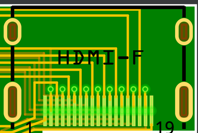
Awesome! Thank you for your help! Another part I am having trouble with is this Female HDMI connector. When viewing the Gerber it does not drill out the “oval” slots. Do you know why?
DIP - 20 pins.fzpz (8.9 KB)
For non-circular holes, you can make cutouts in the PCB
I’ve posted how to do it (search…)
You can make them the shape you want - I did a quick example showing only one rectangular cutout (didn’t bother to Radius the corners, which would be needed unless laser cutting).
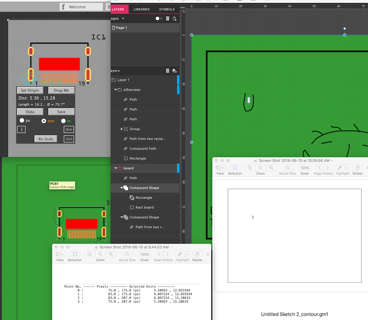
The image below shows Example of:
• Using Woof_App to get location of the desired pad location (shown with lower left Pad though I made the cutout for the upper left pad - too much morning coffee!). Woof App is also posted, (search…)
• Printout of Woof Data for corner points of pad
• Creating the Cutout (using Gravit but, you can use Inkscape / others). Also penned some ink around it for silkscreen example
• The resulting cutout shown in the Gerber’s Contour file
Ability to actually produce a non-circular cutout depends on who makes the pcb and equipment…
Thanks opera_night. I actually added the holes into the custom PCB board shape.
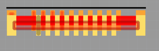
On that last part that I attached (DIP - 20 pins.fzpz) when the gerber is viewed the pads are the wrong size. Any rectangle that I have used in my custom parts is enlarged. You can see in the picture that the pads form a solid copper connector.
You’ve most likely discovered the ‘Fussy-ness’ of Fritzing and making Parts & PCB’s…
It does take a good bit of working with to understand the workarounds to getting what you want. But, you can get there.
( An aside comment) Personally, after ‘getting there’ with Inkscape, I discovered easier-to-use drawing apps and couldn’t delete Inkscape from machine fast enough!
But, ALL drawing apps I’ve used have Quirks requiring time to figure out… Not a perfect world.
Regarding your last post/issue - consider these comments:
• Correct Layer Order
• Correctly ‘Differenced’ or ‘Subtracted’ features
• Correctly made Paths
• Correctly ‘Scaled’ features (depends on DPI export and design values of feature size)
• The big Red rectangle results from incorrect aspects of the above (been there a million times with similar results). That, in addition to a few other ‘head-scratching’ quirks.
Never saw Big-Red for “PCB” but have seen it many times for ‘Parts’ and the Part’s PCB svg. Attending to the above corrected it.
Can’t make cutouts in Parts only can do it in PCB (not the PCB of a Part)