Hi, after 6hours of trying to create a part, I give up. I can’t get it done. Can anyone create a Microbit EdgeConnector for me? Thank you very much. I want to use it in a course I make and will be shared with other teachers.
Here is the jpeg I adjusted with Photoshop.
Just saw this post after replying in the MicroBit thread. The top block looks to be the edge connector itself, but I’m unclear on what the headers are meant to do. It looks like the middle set might be for .1 jumpers (or two connections to each MicroBit pin). It isn’t clear to me what the 3 sets of headers on the bottom do though. The .fzz file in the MicroBit thread is a breakout board that uses the Microbit part to do something similar to what is done here. It has mounting holes for the board and holes to allow the Microbit to be bolted in with plastic strips so it can’t fall out or be removed without tools. If the form factor doesn’t suit I can change it easily enough (such as if your mounting holes need to be in a specific place for something). Here is an image of the breakout board that I have cut as boards:
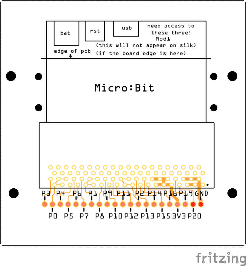
As noted the top section of the silkscreen is truncated by the board edge and doesn’t appear on the board. As noted the 4 M2 holes beside the MicroBit secure a plastic square beam bought from Ebay and cut down to hold the Microbit in place so it can’t vibrate out of the socket if used in a robot. You (or I) can modify the fzz file to add more connectors if you need them, the MicroBit part itself shouldn’t need changes and fits the listed Adafruit connector (I expect it will fit any MicroBit connector, but I have only tried the Adafruit ones). You should be able to add a 21 pin header .1 outwards from the current connectors to the socket via the fzz and either connect them with jumpers or put a trace between them depending on what is intended (you may need to change the position of the text though, but that can be done in the sketch). Then add and connect the extra headers in the jpeg with standard header parrs in the sketch and connect them as desired. If you need a narrower PCB, you can modify the sketch. The part ends at the M2 screw holes and so is pretty much the minimum space needed for the edge connector. You can move the board edge down as far as the pads of the edge connectors and the holes and silkscreen should be truncated as outside the board boundary (although I haven’t tried that).
Peter
Hi Peter
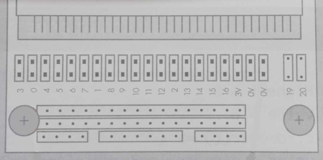
When the thick orange lines to GND and 3V3 are erased and P19 and 20 is changed to GND, it’s what I need. Pin 19 and 20 are not being used. Also the GND on the image you uploaded is not on the Microbit. Just look at the image I uploaded.
If you could do that I would be really grateful. Time is ticking. My course must be finished by monday.
I’m still unclear on what you need although a modification should only take a couple of hours once I figure out what you want. The thick lines are there to provide low resistance for the power lines. A number of the MicroBit pins use 4 pins on the edge connector as the part shows. The part as it stands correctly connects to all the pins on the Microbit (I have a couple and have tested it). I think what you want is to move the ground pin to where 19 is now, and delete pins 19 and 20 (although they are on the MicroBit and I would suggest leaving them perhaps moved to to after the ground. This can also be done with the current part by just adding the connectors you want and connecting them to the pins on the current part. The downside to that is that there will be an extra line of pads if space is an issue.
Peter