I’m looking for a way to create fancy looking faceplates for a synthesizer using PCB. Since Fritzing does not have editable layers, modifying the copper layer or solder mask layer is a challenge.
I have two questions:
Any idea if it’s possible to add svg graphics to the solder layers?
Is it possible to modify the solder mask, so the copper is seen through?
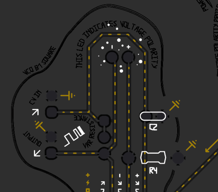
Here is an example board design:
Bottom copper - connecting all components
Bottom copper - the black lines are also on that layer. They don’t touch the actual components, but they are visible.
Solder mask - where you see gold lines, that’s the top copper layer is visible
Yes. If you create a custom part. The copper layer is an svg.
There are a couple of ways. Most flexible is to make a second copy of the sketch which creates the solder mask layer you want, then substitute the solder mask layer from that gerber output with the solder mask layer of the actual board you want. The second method “invisible copper” (a copper layer with fill=none) fools the mask creation code to not put solder mask where there is “invisible copper”. That method is described in this forum post.
@vanepp thanks for the tip! It sort of worked, but I’m not sure how to make the graphics visible in the copper. Do I have to define the copper sections of the custom part as “connectors” to make them visible? If so, is there a way to select them as a group, or do I have to do it manually?
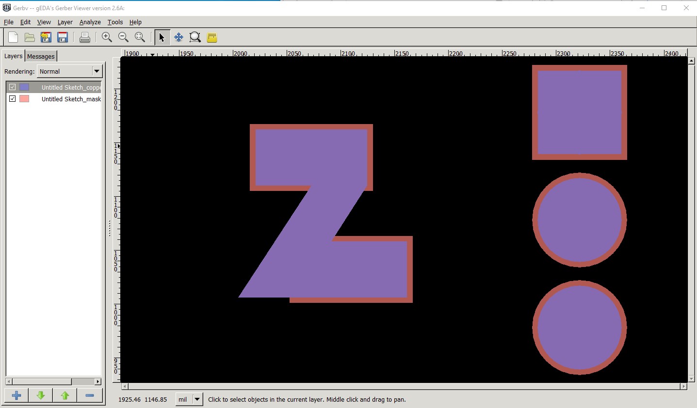
No just the pads on the copper layers should do the trick. Here are a couple of examples (they have connectors because I cloned a fc-51 part, but they shouldn’t be needed) and their gerber output
This one has the Z on both sides of the board (the orange outline is the mask layer in the gerbv gerber viewer
This one has the Z only on the top (between the copper1 and copper0 groups.) If you are doing a no connectors one I would use copper1 only as an SMD part (although that isn’t the case here.)
here the three pads are on both layers the Z is only on the top layer. Unzipping the .fzpz files and looking at the associated .fzp file should tell you what to do.
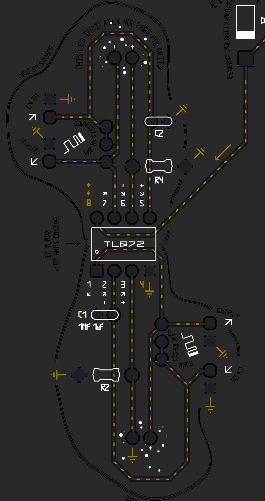
Hey @vanepp thanks again for the help earlier. Hope I can bother you with another question on the topic.
In the image below, the black lines indicate copper lines under the solder mask. They are not connected to anything. Only drawn to illustrate certain concepts. Can this also be done somehow?
Yes, but it is more difficult. The mask covers everything that isn’t copper in a part but there is no way (that I know of anyway) to specify mask. So to do this you would need to make a sketch without the copper marked in black, produce the gerbers and save that gerber mask file. Then you output the sketch with all the copper in place as gerbers and substitute the first mask file in the latest gerber output which will cause the black copper to be under the solder mask because it wasn’t copper in the first sketch and thus didn’t get unmasked.