I have been trying to build the PCB svg for the SOT-89 version of the MCP-1700 fixed voltage regulator. I have had interesting problems.
First, I used the layout suggested in the data-sheet:
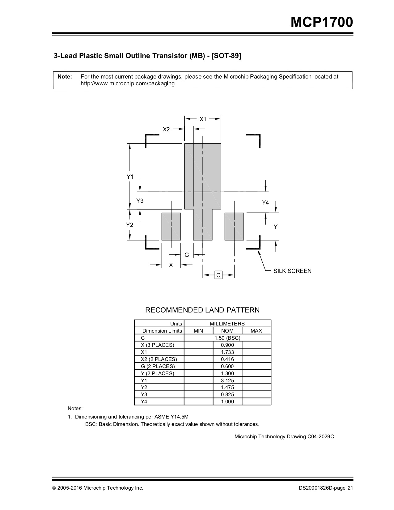
I hand edited the PCB, scg file. Starting from a SOT-89 transistor.
I had to make some adjustments, because it seems that Fritzing doesn’t like pads so close to the edge of the device definition, nor pads so close to each other.
Three issues remain.
First, I don’t know how to deal with Pad2, which is the sum of two rectangles.
Also, I get the following errors, which I don’t know how to deal with:
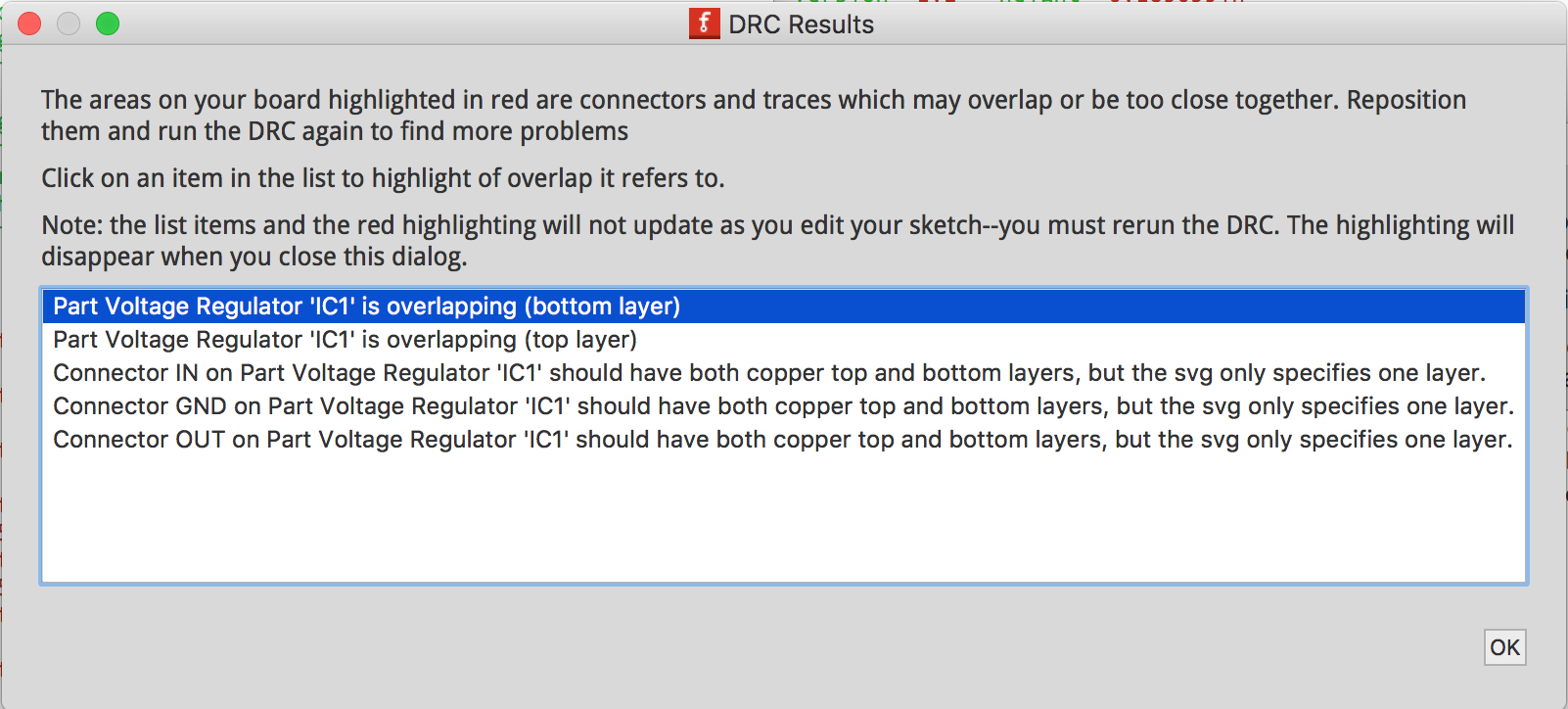
The first two error lines have to do with the two touching rectangles that represent pad2.
I know this because if I comment out one the rectangles, that error message goes away.
Second, the next three lines in the DRC report I don’t know how to resolve – the part is an SMD part, so the PADs should only be on the “top” side. So they are in the copper0 layer. The copper1 layer is empty. What I am missing?
Third, when I associate pads with connectors, I can’t click on the rectangle, if the silkscreen layer is there. The silkscreen layer seems to be above and obscuring the copper layer.
Does anyone have experience designing an SMD part, who has seen these error messages?
Attached is the part
allan Voltage Regulator.fzpz (5.9 KB)