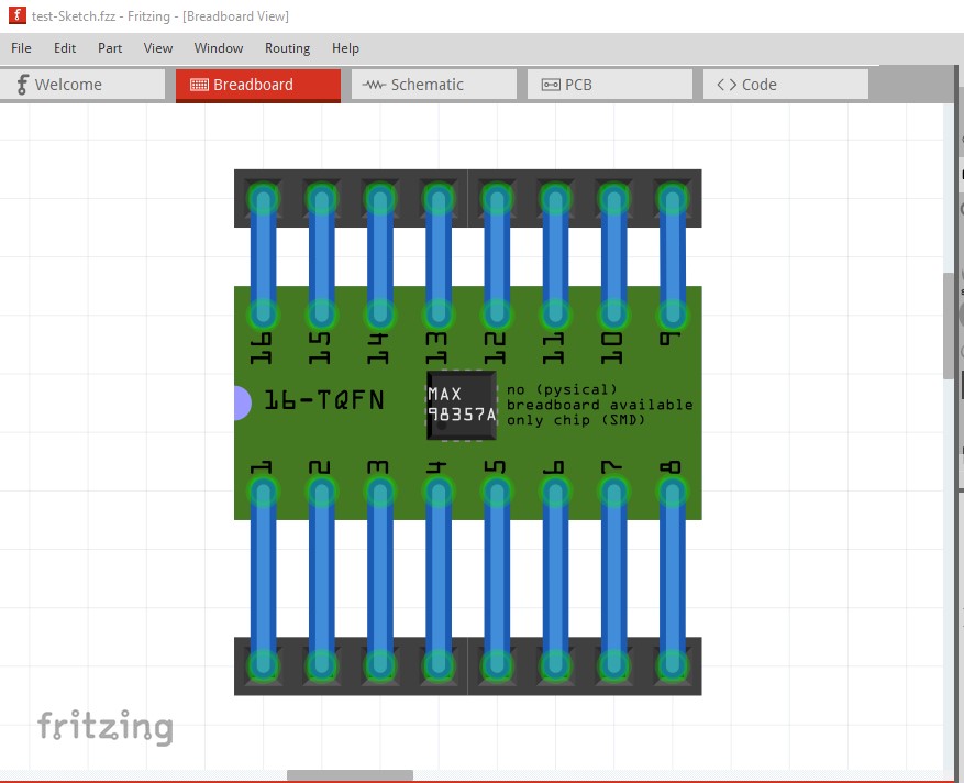
Typically the carrier board in breadboard is green like this (although it doesn’t make any functional difference!)

More serious is an error in the fzp file where
<pcbView>
<p layer="copper1" svgId="connector14pad"/>
</pcbView>
</views>
</connector>
<connector type="pad" name="BCLK" id="connector15">
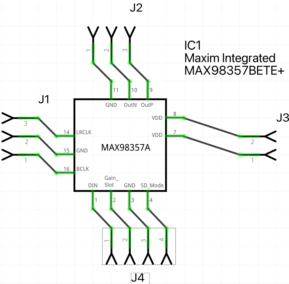
<description>BCLK (16) Bit Clock Input</description>
<views>
<breadboardView>
<p layer="breadboard" svgId="connector15pin"/>
</breadboardView>
<schematicView>
<p layer="schematic" svgId="connector15pin"/>
</schematicView>
<pcbView>
<p layer="copper1" svgId="connector15pin"/>
</pcbView>
should be
    <pcbView>
      <p layer="copper1" svgId="connector14pad"/>
    </pcbView>
  </views>
</connector>
<connector type="pad" name="BCLK" id="connector15">
  <description>BCLK (16) Bit Clock Input</description>
  <views>
    <breadboardView>
      <p layer="breadboard" svgId="connector15pin"/>
    </breadboardView>
    <schematicView>
      <p layer="schematic" svgId="connector15pin"/>
    </schematicView>
    <pcbView>
      <p layer="copper1" svgId="connector15pad"/>
    </pcbView>
(connector15 pin should be connector15pad to match the svg file) which causes no connection on pin 15 in pcb. As well schematic needs a terminalId like this:
<connector type="pad" name="BCLK" id="connector15">
  <description>BCLK (16) Bit Clock Input</description>
  <views>
    <breadboardView>
      <p layer="breadboard" svgId="connector15pin"/>
    </breadboardView>
    <schematicView>
      <p layer="schematic" svgId="connector15pin" terminalId="connector15terminal"/>
    </schematicView>
Fritzing loads parts by its own rules (mostly undocumented.) It is up to you to place and rotate them as desired.
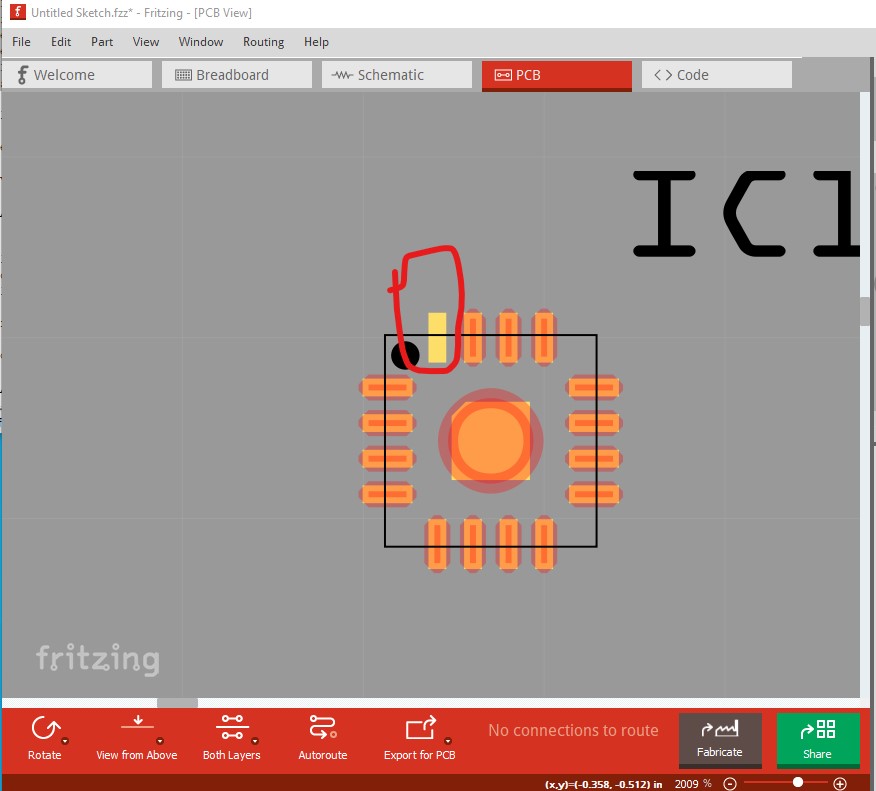
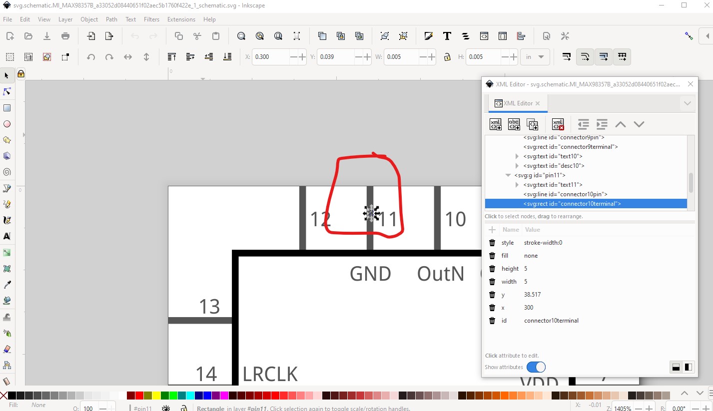
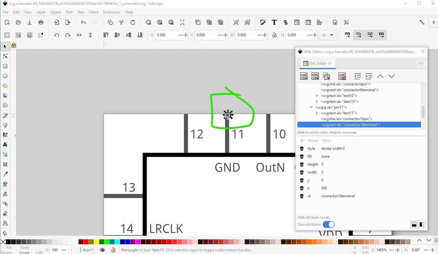
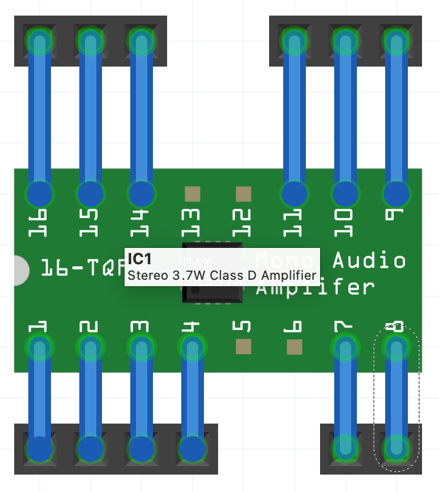
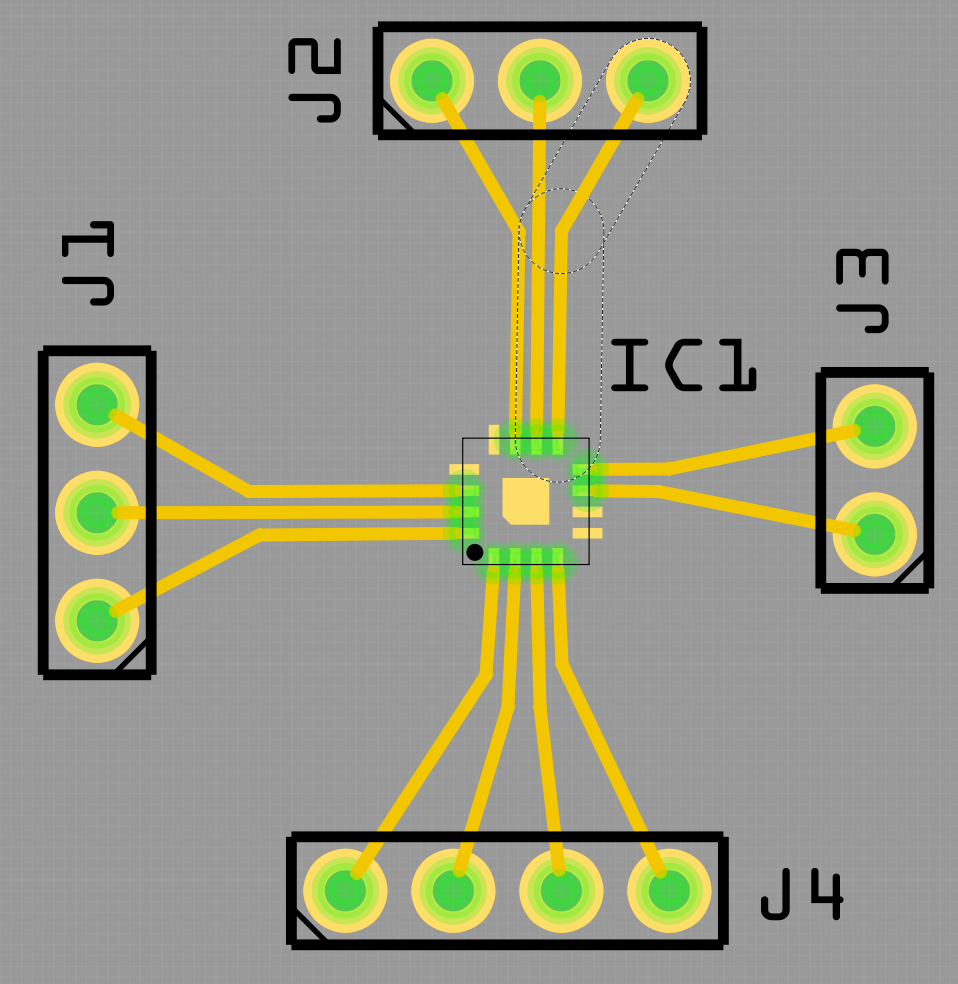
It doesn’t have a connector defined so it won’t connect to anything I don’t think. However thermal pads usually want to be grounded so this one may need to have a connection defined for it (I haven’t looked at the data sheet though.) In addition there are another couple of problems that show up in testing. In the schematic svg the termninalId is in the wrong place on connector10:
It needs to move to the top of the pin like this
as noted above connector15 lacks a terminalId definition in the fzp file and thus the wire connects in the middle of the pin like this
as well the connector in the svg is mislabeled so even when the fzp is fixed it is still incorrect
both corrections are needed for it to work correctly.
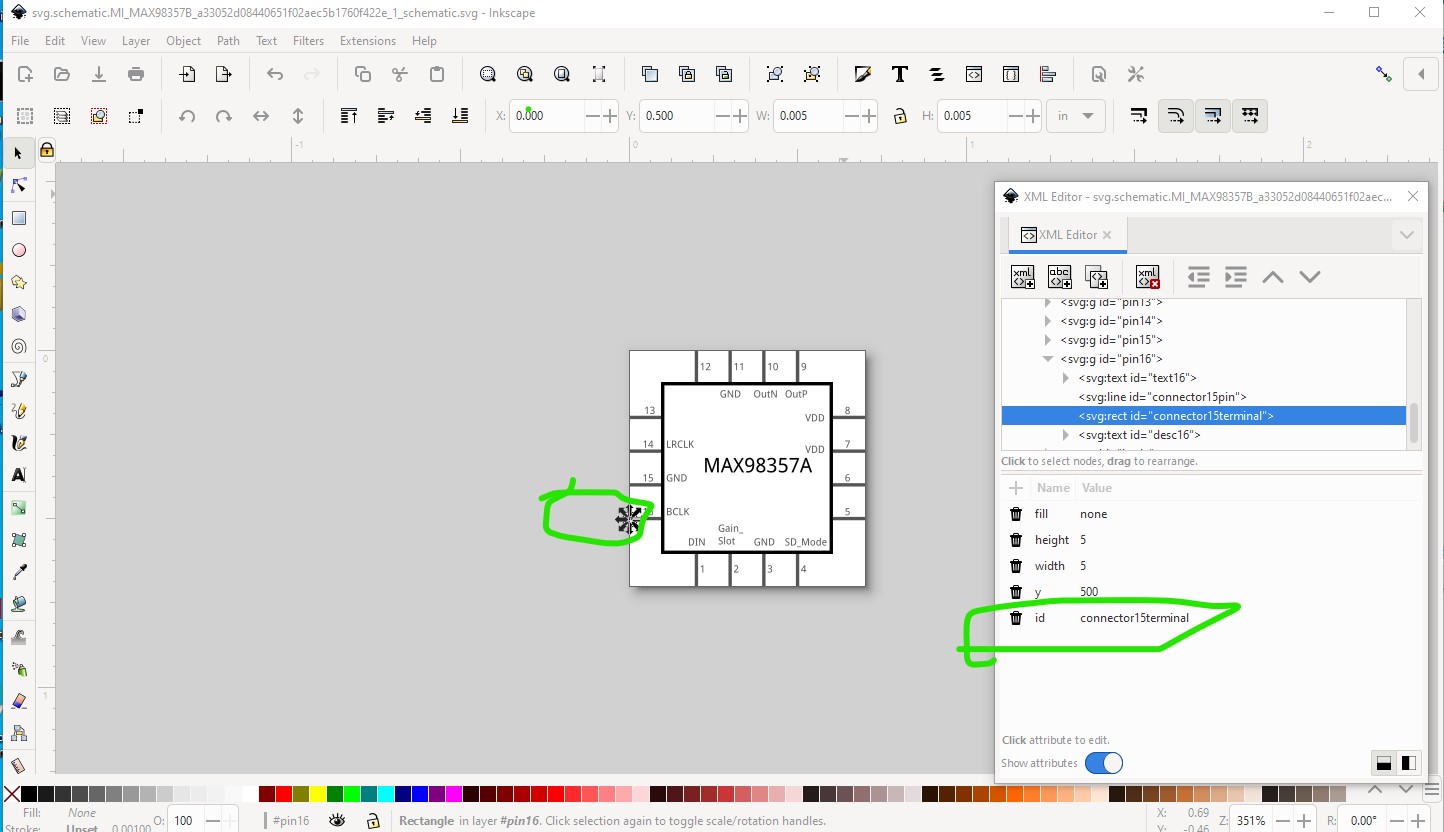
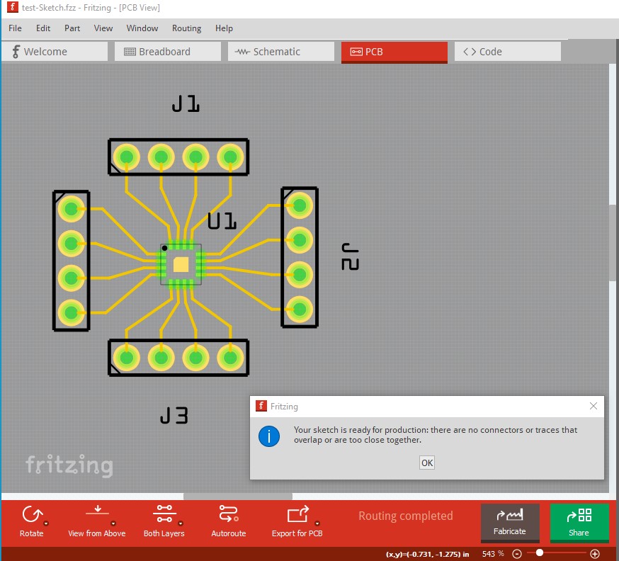
with these changes the part now works correctly:
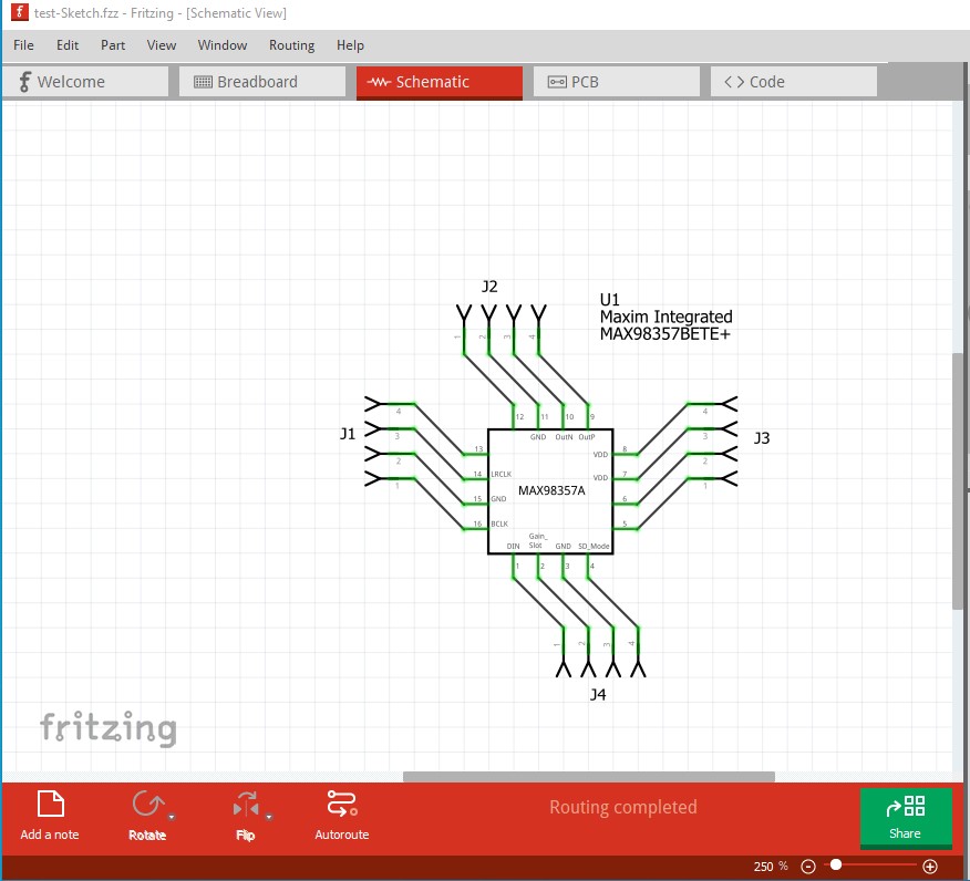
. and passes DRC. These images were generated from this test sketch
test-Sketch.fzz (20.2 KB)
which is what you should make and check before posting a part.
Peter