Not a bad part, but it has an error. The pcb svg has ellipses instead of circles and thus the holes are not drilled in the gerber output. The gerber drill.txt file
; NON-PLATED HOLES START AT T1
; THROUGH (PLATED) HOLES START AT T100
M48
INCH
%
T00
M30
is empty meaning no holes. I knew to look for this by running your part through FritzingCheckPart.py (which can be found in this tutorial on parts making)
which produces this output (edited for size!)
$ FritzingCheckPartw.py ‘part.MAX7219 32x8 LED Dot Matrix Display_c7830f5cafd7c607a76591ec76457968_5.fzp’
**** Starting to process file Startup, no file yet
**** Starting to process file part.MAX7219 32x8 LED Dot Matrix Display_c7830f5cafd7c607a76591ec76457968_5.fzp
**** Starting to process file svg.breadboard.MAX7219 32x8 LED Dot Matrix Display_c7830f5cafd7c607a76591ec76457968_5_breadboard.svg.bak
**** Starting to process file svg.schematic.MAX7219 32x8 LED Dot Matrix Display_c7830f5cafd7c607a76591ec76457968_5_schematic.svg.bak
**** Starting to process file svg.pcb.MAX7219 32x8 LED Dot Matrix Display_c7830f5cafd7c607a76591ec76457968_5_pcb.svg.bak
File
‘part.MAX7219 32x8 LED Dot Matrix Display_c7830f5cafd7c607a76591ec76457968_5.fzp.bak’
This is a through hole part as both copper0 and copper1 views are present.
If you wanted a smd part remove the copper0 definition from line 47
…
Error 65: File
‘svg.pcb.MAX7219 32x8 LED Dot Matrix Display_c7830f5cafd7c607a76591ec76457968_5_pcb.svg.bak’
At line 104
Connector connector0pin is an ellipse not a circle, (gerber generation will break.)
Error 74: File
‘svg.pcb.MAX7219 32x8 LED Dot Matrix Display_c7830f5cafd7c607a76591ec76457968_5_pcb.svg.bak’
At line 104
Connector connector0pin has no radius no hole will be generated
Error 65: File
‘svg.pcb.MAX7219 32x8 LED Dot Matrix Display_c7830f5cafd7c607a76591ec76457968_5_pcb.svg.bak’
At line 105
Connector connector1pin is an ellipse not a circle, (gerber generation will break.)
Error 74: File
‘svg.pcb.MAX7219 32x8 LED Dot Matrix Display_c7830f5cafd7c607a76591ec76457968_5_pcb.svg.bak’
At line 105
…
which corresponds to this in the svg (here displayed in Inkscape, which looks to be what you are using):
Here we see there is an rx and ry (and the element is labeled ellipse not circle!) rather than a r
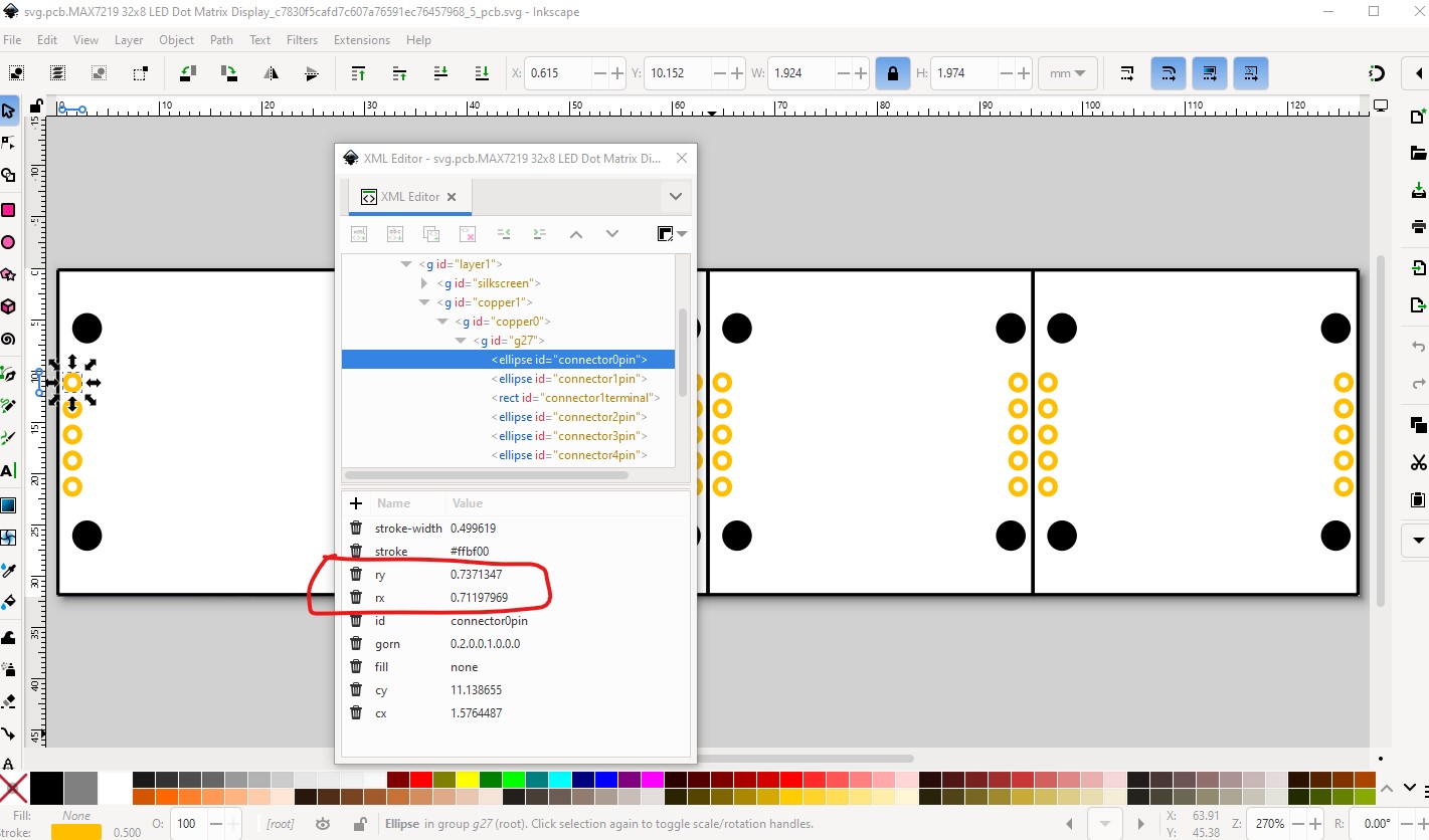
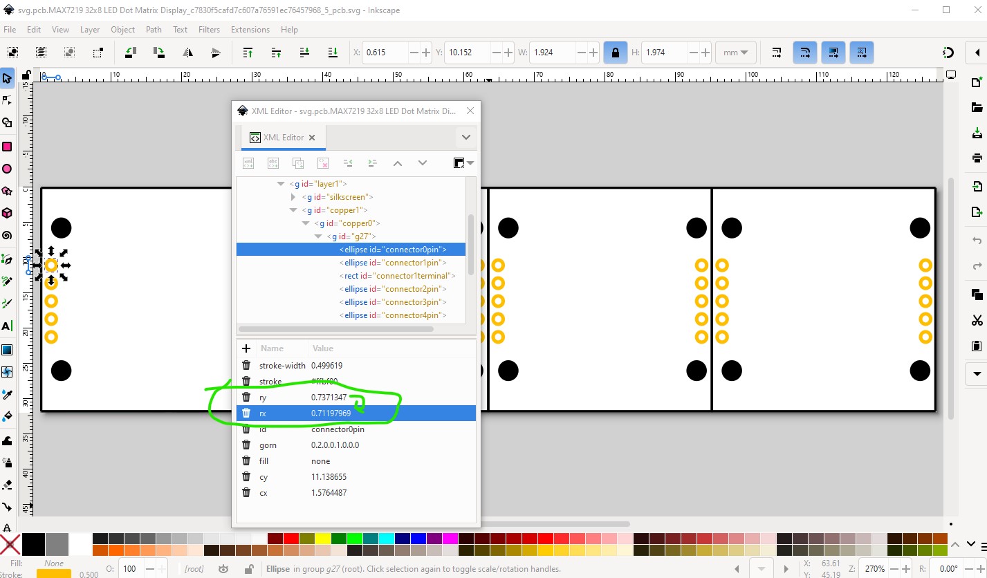
to fix this copy rx to ry like this
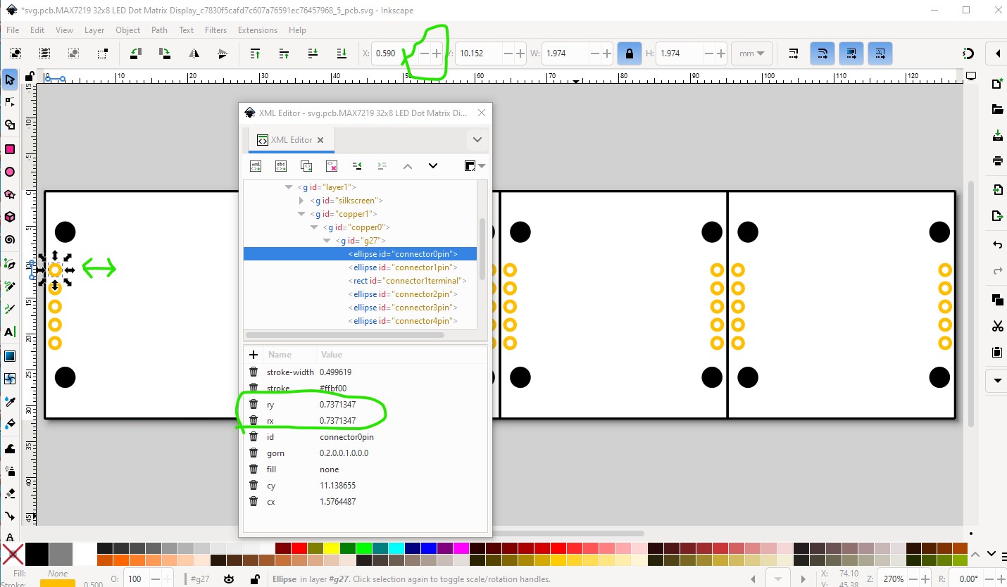
That still hasn’t fixed it, just enabled the fix. To change it to a circle from an ellipse you need to move the pad one position left then right with the tool bar like this
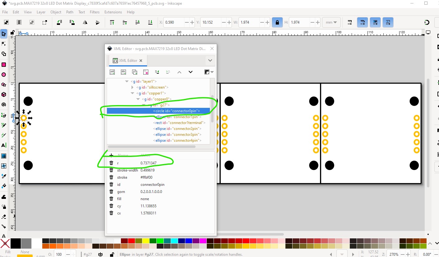
The pad ends up in the same place it started but has been converted from an ellipse to a circle in the process. Unfortunately you need to then do this one at a time for all the rest of the pads, I don’t know of a way to do this as a group (if anyone does please post it!) which is a large pain, but at least this works if with a lot of work. That will then generate the holes in the gerber output. Hope this helps!
Peter