A small problem for me, but perhaps a big opportunity for Fritzing in the ever-growing SMT/SMD world—connectable PCB pads. I often have SMD parts for which no Fritzing part is currently available, but I could create one on-the-fly with the sizeable pads in PCB view, except they have no connections and do not show in the schematic view. If the pads could be circuit-connectable, then any part or device footprint could be created as-needed, without every user having to learn to modify existing parts or create new ones. With dozens of new or unique SMD footprints coming out weekly, a solution is necessary to allow Fritzing to be useful and flexible with that growth.
I am currently having to add a test point on-top of pads to make them appear in the schematic (e.g., antenna connection), but that’s clumsy and messy. Is there a simple option already available, or can schematic-connectable versions of the PCB pads be developed?
Yes, I am doing that now, using test points stacked with pads. Effective with only double the work. Imagine how much simpler it would be to create some of these oddball SMD footprints (and other non-SMD terminations) if the pads were connectable and showed in the schematic? How are you making all these SMD parts that are likely single-use yourself?
BTW - the frame of mind for stuff like SMD is that they are footprints, not “parts”, and will not be obsolete in the next iteration. We have generic DIP8 parts for THT, and can feasibly use them for everything DIP8, typing the connections and other info as-necessary. This holds even more true for SMD, where they are all package footprints, and most common ones are exactly that designation, such as 0805, SOT-23, etc. Imagine the flexibility of creating oddball (or even common but unavailable) SMD footprints on-the-fly as you need them. Awesome.
I literally make at least one new one-off part per week. If I need a 0.650" resistor I pull the svg, move the nodes, put it back in, and 3 min latter bang it’s done. Then I share it to help the community. You have to make the decision to remake and move separate pads for the rest of days, or learn how to make parts.
By the sounds of it this video is all you need.
FZ is not really SMD ready, because it was never intended to be high end, it’s just that people like it so much they are slowly making it better.
I noticed that SMD has different names for similar footprints, so if the footprint doesn’t come up in a search just pull components in PCB view until you see the correct one.
Here is a car EMS using SMD, and also using my DENSO and MPX sensor parts that used to be individual header pins and holes, without silkscreen outlines, from the CORE parts bin.
I apparently touched more than one nerve and I apologize if my enthusiasm for a simple feature that would greatly increase Fritzing’s usefulness has clouded the question, and sent the conversation off-track. I thought the various “why” examples were of interest but are in-fact irrelevant to the answer I am seeking, agreed or not. Back to my question: Can PCB view pads have a connector permanently attached to make them connectable in schematic view? Thanks
Just going through my KiCad, and it doesn’t seam to exist. Net search and it doesn’t seam to exist either. Net recommendation is to make a part or use netlist.
A bit of a Eagle search, and it doesn’t exist either. Recommendation use netlist.
Awesome! We could be one of the first few to make it available. Thanks for your answer. Now, does anyone know how to attach a connector to the pad part so it shows in schematic view?
Sorry it’s never going to happen, like in all other EDAs, because it serves no purpose.
What you are saying is you want floating pads to represent a part. How are you going to show that it is a part, or even label it and give it values so it doesn’t get mixed up with other floating parts in a circuit.
Like was said, either make the part, use netlists, or even worse is make a floating pad part, which you will have to remake every time you need to change size because created parts can’t be made to be adjustable.
Can anyone answer my question? Old gray is so defensive about parts-making, that he cannot see answers to his own questions that are simple to see if not so biased, and avoids answering my question for personal cause. Blocking assistance rather than helping to look for solutions. To reverse the point - what is the reason for pads that cannot be connected into the circuit so they can be seen? As they are connected, they should be viewable. SMD footprints for one-use parts is just an afterthought that I thought could be useful. I am already using workarounds, and it’s great. But could be much better. Please, can anyone just answer the question - how to attach a connector to the pad part so it shows in schematic view?
The pad does not have a schematic .svg, so there is no way to make it appear in the schematic view. One why is to overlay the pad on a single pad connector and have one pin in the schematic view. Although that is kind of counter productive and you probable have already tried that… The only other way I can think of is to create a one pad part… each pad would have one schematic pin… the breadboard view could be left out if you want. The problem is that the pad is not adjustable, therefor you would need to make a bunch of them with different size pads… once you had all the different size pads made up it would not be to difficult to drag on to the board to make a footprint…
If it were me, I would setup a parts factory on a graphics editor. It would be difficult to do in Inkscape, but AI or CorelDraw it would not be that difficult. Just make a series of pre-made pads and pins and save them on a page then drag them on the a parts page and create an instant part without using FZ parts editior. The problem is that it takes a little bit of a learning curve to get to that point where you can make parts ready to go efficiently.
Excellent! Thank you. If I understand correctly, due to some Fritzing program internal dynamics, the pad function loses the sizing ability if a connection is added to it? If so, that would be a poor exchange of overall benefits. And, no way to add connect-ability without also losing that pad-sizing ability? If so, that rather kills the usefulness of the sizeable pads. Catch-22 it seems. Thanks again for your response, and I will look into making a ‘parts factory’!
Not exactly… I believe “pad” is generated by some kind of a script… maybe one of the python scripts… I wouldn’t really call it a part. It generates one connector (connector0pad) in the PCB view.
A Part generally consist of 4 files (part.fzp, part_breadboard.svg, part_schematic.svg, and part_pcb.svg). There are a lot of tags that can be uses in the .fzp to allow the part to do things like allow it to rotate or flip or not to rotate or flip… among other things. I just don’t know what they all are. There may be one to allow the part to be sizable… maybe, maybe not, I just don’t know what it would be. I tried a bunch of experiments one time, like “size, sizable, (true), etc.”. I couldn’t fine anything that would work. Maybe one of the core people can answer that question…
A part .fzpz in just a zip file. You and unzip it to get a better understanding on how they work…
@AlanChenm thanks for that, and indeed that is what I have been using under pads to make them connectable, as described in the first post.
In the meantime, if developers are interested in the concept I also wonder if the mechanism to make ground fill is a pathway? They are of course sizable to various dimensions and connectable. Dev’s?
 Imagine how much simpler it would be to create some of these oddball SMD footprints (and other non-SMD terminations) if the pads were connectable and showed in the schematic? How are you making all these SMD parts that are likely single-use yourself?
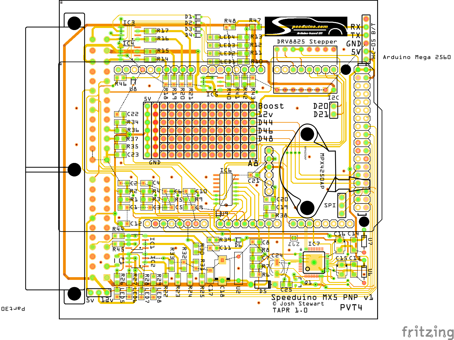
 Thanks for your answer. Now, does anyone know how to attach a connector to the pad part so it shows in schematic view?


