This is darn-near the coolest discovery…. 
It turns out that making a contact pad with a Rectangular cutout is very easy.
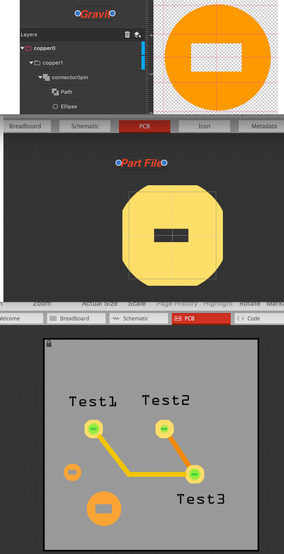
In previous post’s I referred to making simple cutouts using SVG’s ‘intrinsic’ ability to ‘Difference’ elements.
Example (the SVG):
I created the usual two layers; copper0 & copper1
I created a filled circle.
I created a Rectangle by drawing 4 bizer lines in a CounterClockwise direction (that’s the key to intrinsic Differencing).
I first selected the Circle then, the Rectangle and Differenced them (thus ending with a Differenced Path).
To test this:
I used a core part (an Antenna). I was not concerned with the Schematic/Breadboard/Icon.
I placed three of them on a PCB.
Also, I dragged two “Copper Image’ parts onto the PCB.
I stretched one of the Image parts to enlarge it.
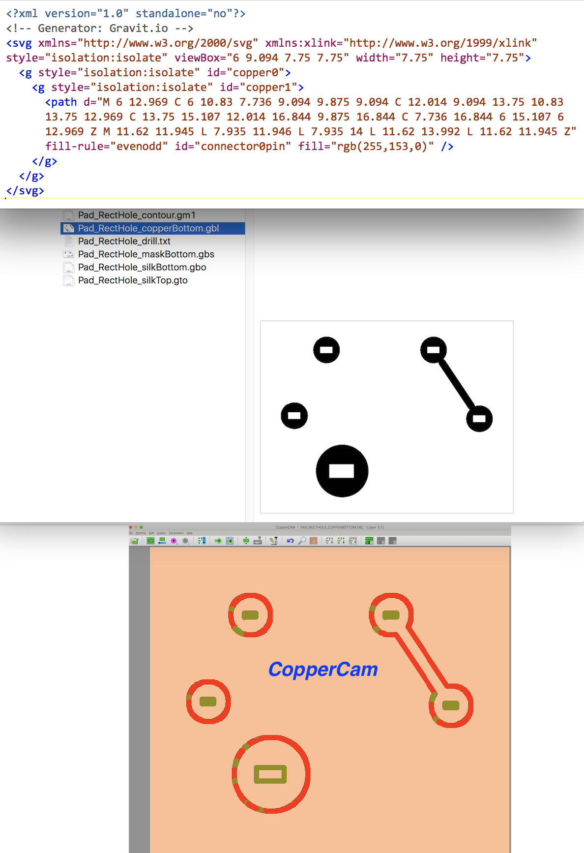
I exported Gerbers.
I loaded them into CopperCam.
Results: It works!
NOTE: Of course, you can’t drill a Square Hole but, you can Mill and Laser it. The resulting Gerbers are enough to enable this via setting them as Contours when setting up the machining files.
Below are files and images…
Fritzing File: Pad_RectHole.fzz (7.9 KB)
The Part File: Pad_wRect_Cutout.fzpz (5.2 KB)
The Pad SVG File (delete the .fzp) Pad_wRect.svg.fzp (663 Bytes)
FYI - I made the SVG in Gravit. I imagine using Inkscape will work…