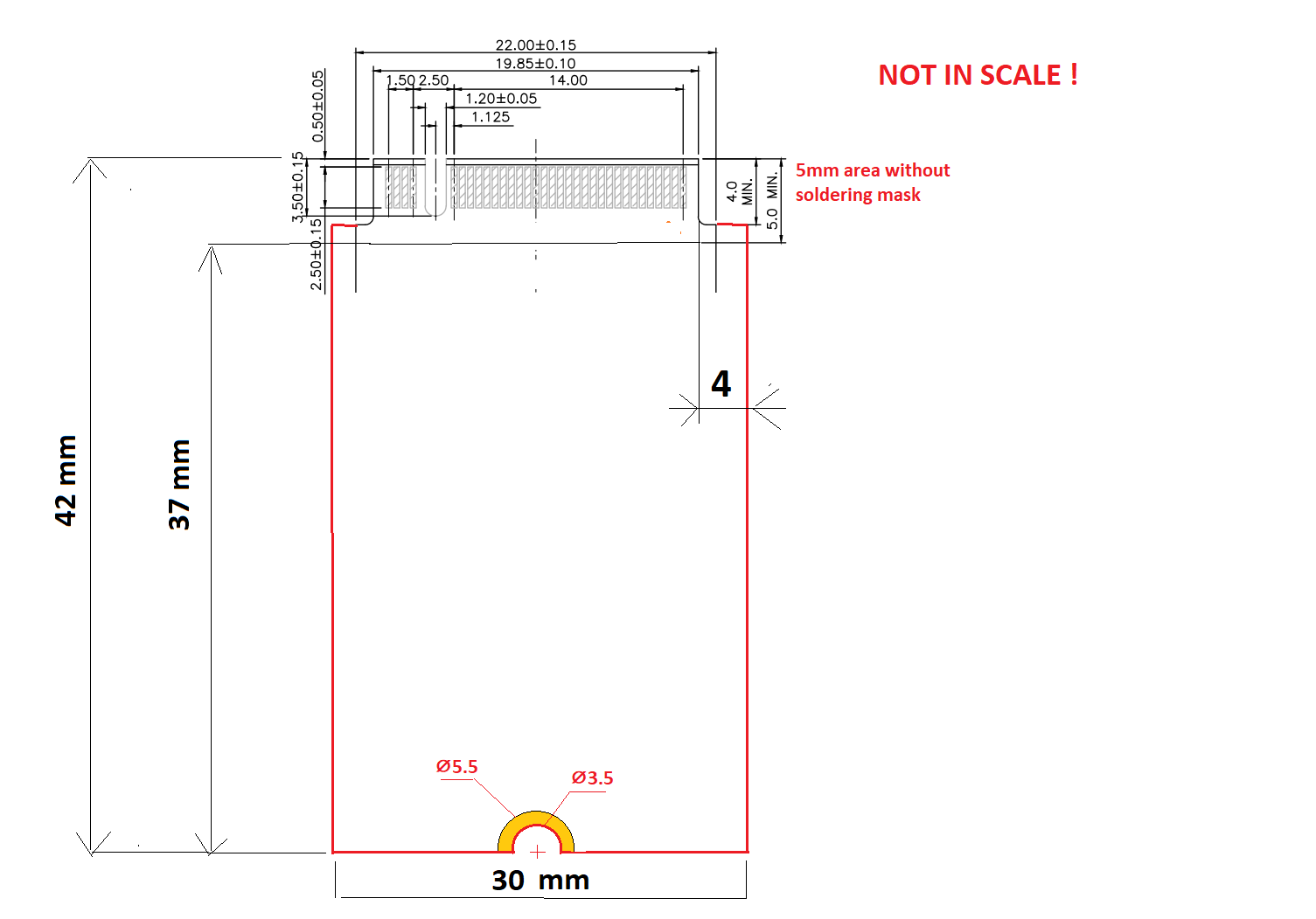
OK here is the board outline for the pcb as a part (which only has pcb silkscreen.) It would be useful to print the footprint out at 1:1 scale and compare it to a real board to make sure the size is correct.
edit
deleted incorrect part!
The slots can be made either by holes as you suggest in the part, although as noted that is suboptimal as the holes can’t overlap because at least some board houses reject pcbs with overlapping holes because the drills break (and presumably cost money with the downtime to replace the drills.) the other option is to do a board outline as for the board which can cut the needed slots, but needs the size of the board (because it will be the outline of the board), and the position of the connector on it (for the location of the slots) but is more work to change if needed as both the outline svg and the sketch need to be updated. I’d guess that we will only get 2holes each 1.2mm dia and likely in need of manual cutting/filing to enlarge the slot when the boards come back. Like this
3 would be better, but likely have the drill breakage problem
depending on the order they drill the holes (I think sequential is likely) the second hole may wander due to not enough board space to start the drill potentially causing drill breakage. You may want to ask the board house you use what their opinion / policy is. The holes are certainly easier from a Frtizing perspective. I’ll continue on with making the edge connectors and the connector part.
edit:
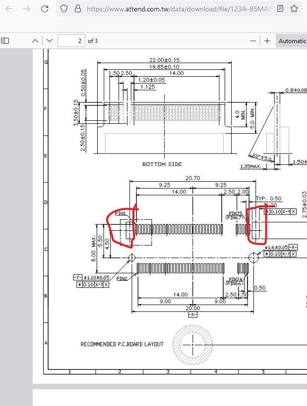
I discovered when I added the connectors this outline isn’t correct. It was made from the first specs above which is only 22mm wide not 33. I’ll use the numbers from the later image which should be more correct I hope.
edit2:
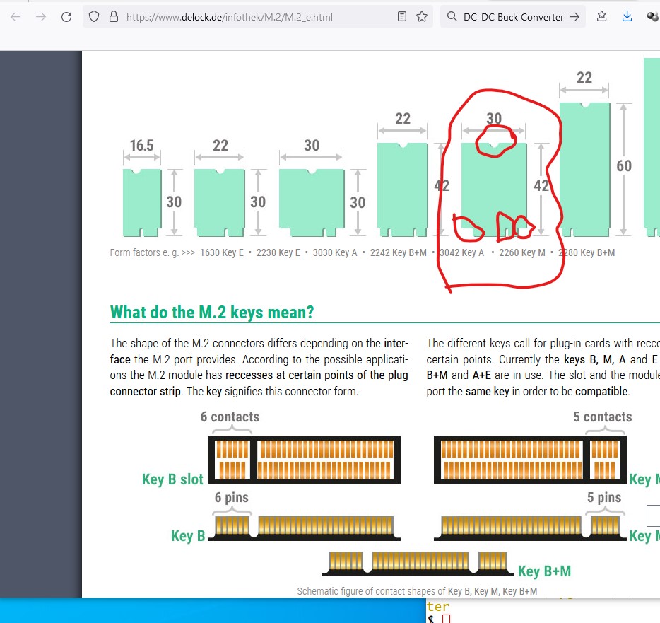
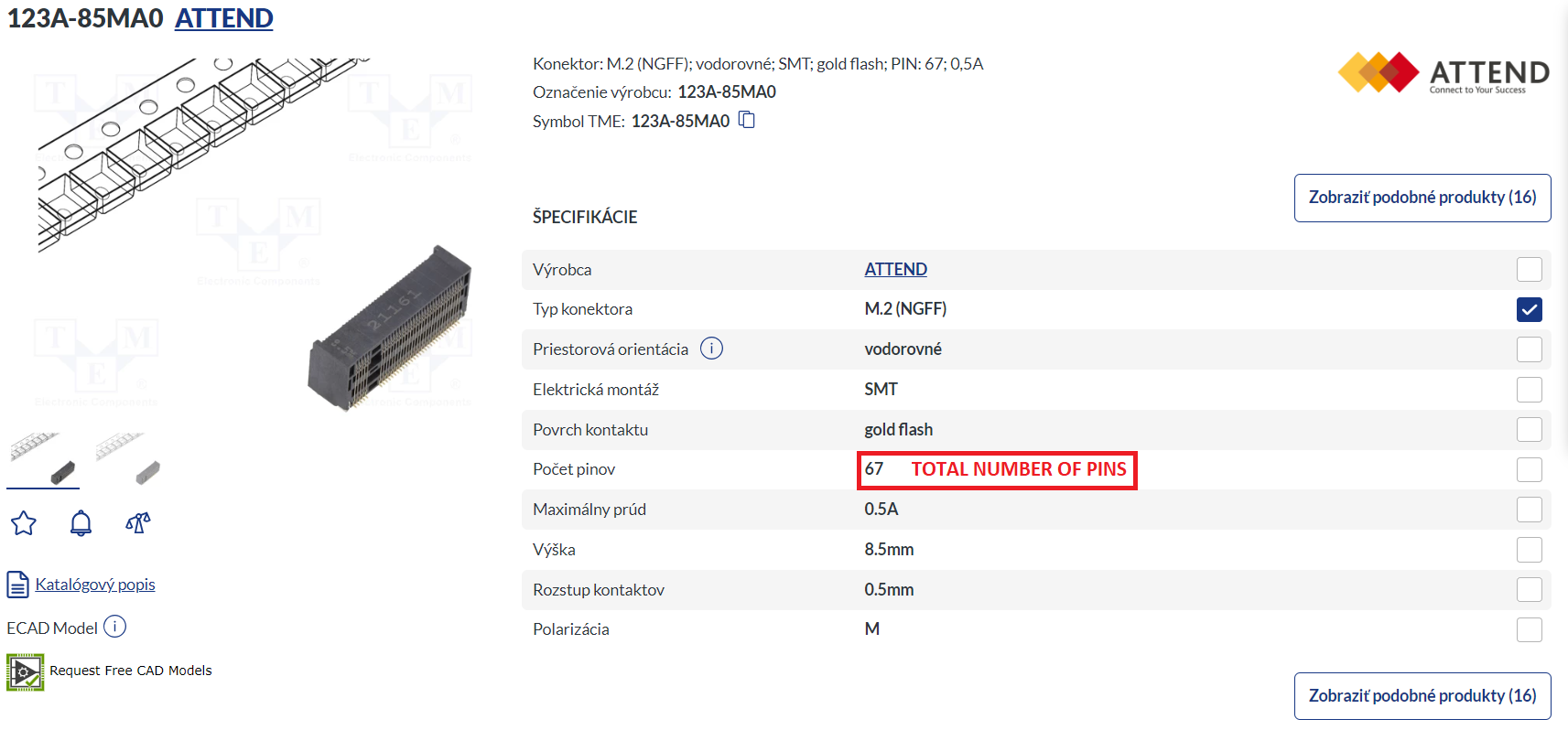
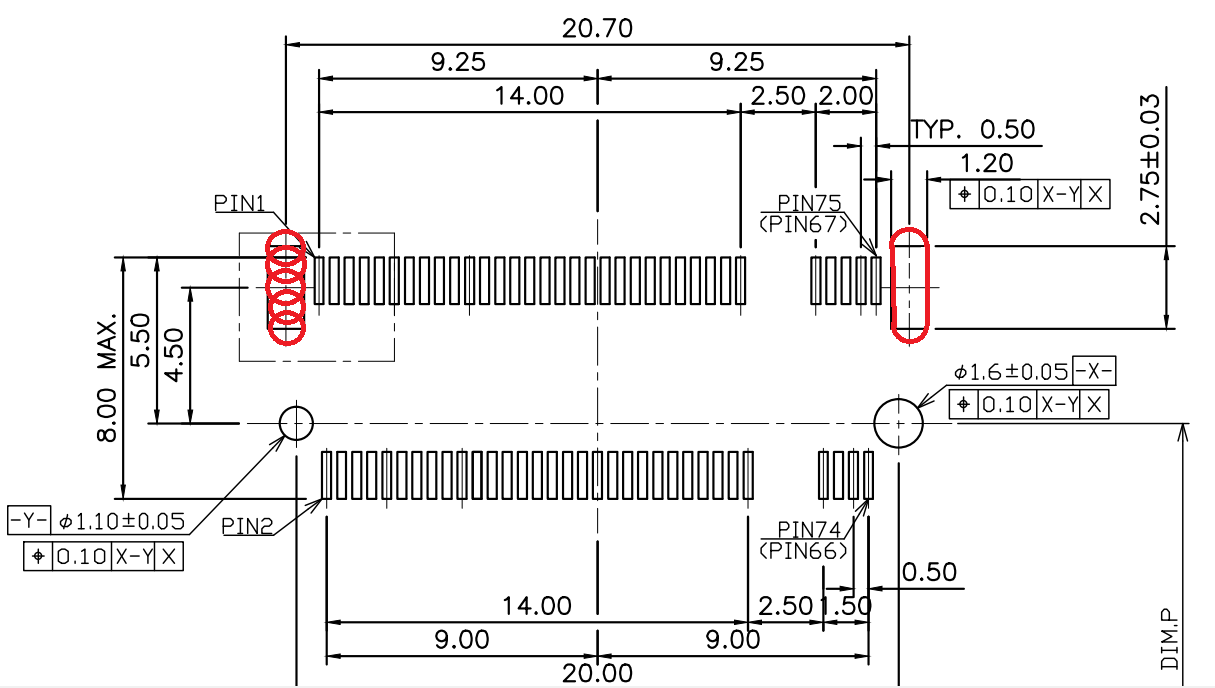
Nope, the pcb definitions are all for 22mm wide pcbs, we need a connector with M key that supports a 30mm wide pcb and has the drawing with dimensions for a 30mm wide pcb. I can’t find one on the Attend web site all their M connectors seem to be set for a 22mm wide pcb which isn’t what we want. I’ll search other sites and see if I can identify anything (but didn’t have much luck last night.) The problem is here (this is the outline.svg for the 22mm size pcb and the connector you requested which doesn’t fit in the available space!)
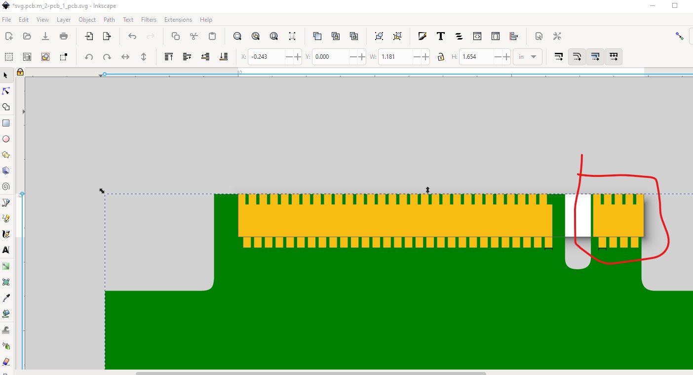
The connector looks a little odd because I offset the bottom pins 0.5mm in y because otherwise they overlap and you can’t see the pins (which will likely be an issue with the part too!) We need to find a connector that has the dimensions for a 30mm wide pcb. As you see the pins on the end circled in red are beyond the board outline and will get truncated and the ones on the right are not positioned correctly I expect.
edit3:
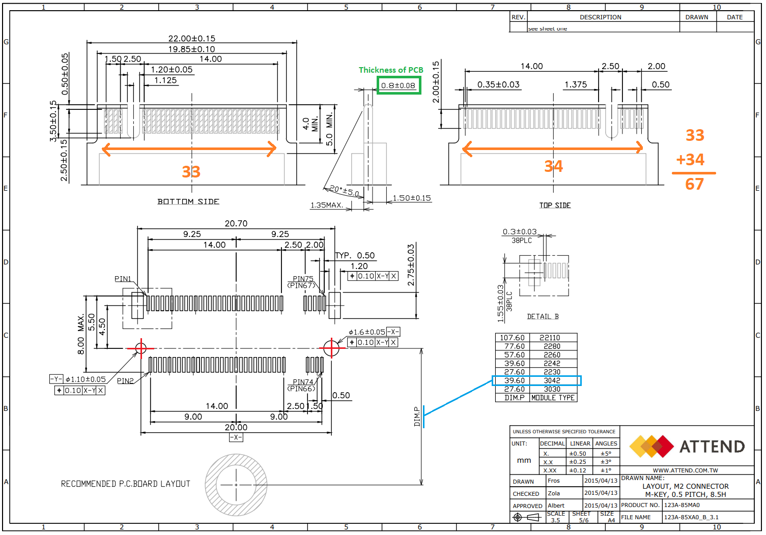
Progress! I found a copy of the M.2 spec here
which has the correct numbers for the outline file, but now there is a Fritzing problem:
the outline file won’t go to the back so the edge connector won’t appear on top of the board outline (which is important because there are alignment lines in the outline.svg which the edge connector needs to line up with to be in the correct position. I’ll poke around a bit and see if I can come up with a solution. Other than that the edge connector appears to work correctly and this should work if we can make the outline go to the back.
edit4:
Fixed! I had misconfigured the silkscreen in the outline.svg file. Correcting that makes it work.
outline.svg (right click and then save image as to download the svg.)

edit5:
replace the fzpz file because I forgot to add the required solder mask blockers to the edge connector …
m.2-pcb.fzpz (12.5 KB)
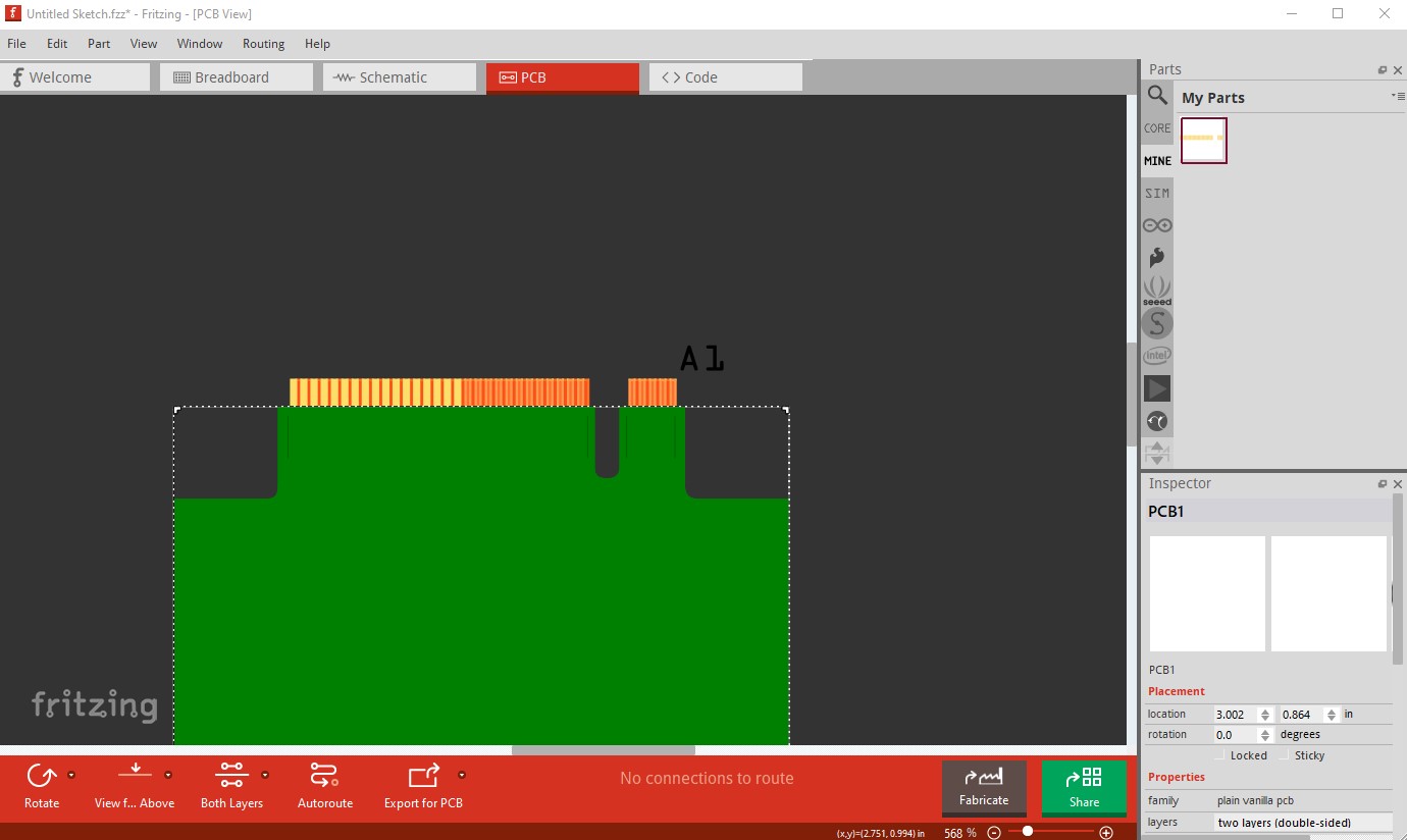
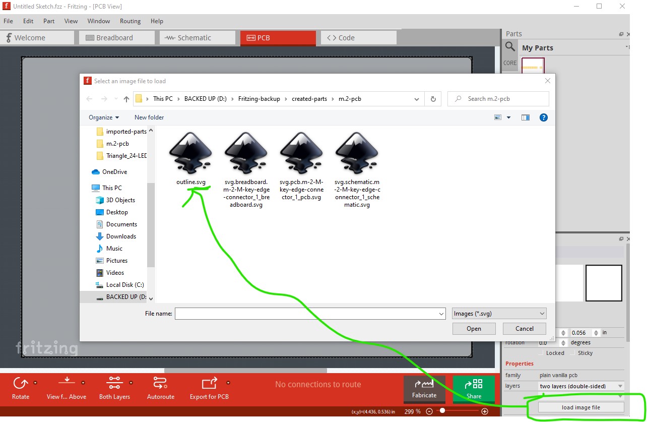
If you click on load image file in pcb, then select outline.svg it will load the outline file like this:
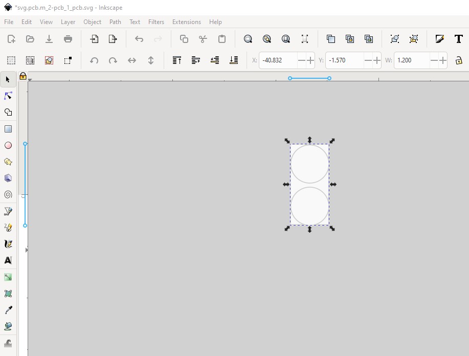
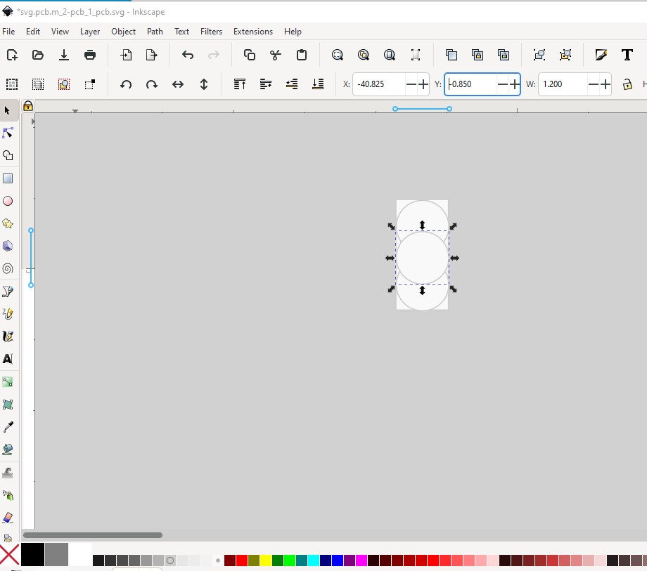
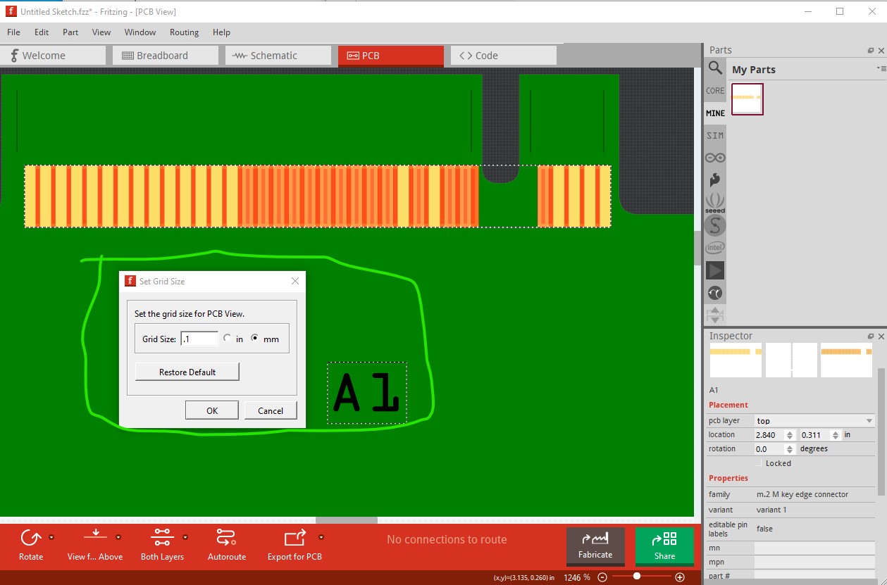
Then you need to drag the edge connector in to the sketch
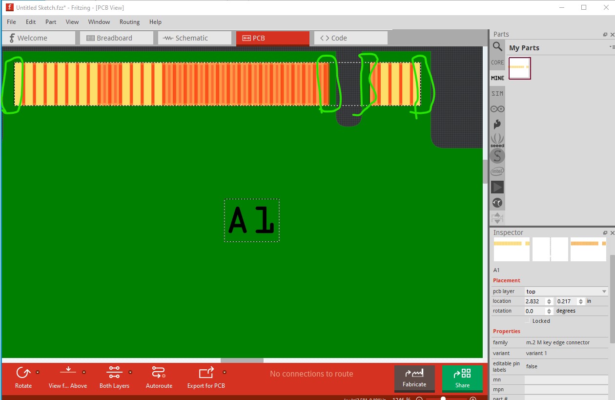
and set the grid size to .1mm then move the edge connector up til it is between the silkscreen lines on the outline file to position it correctly.
That should give you the edge connector in the correct place ready to route. Then comes the connector for the boards but it isn’t done yet.
edit6:
OK here are two parts for the connector. One has 3 holes (which overlap) for the slot and I think the board house may not accept. The other has two non overlapping holes but will require more milling to get the slots correct. I can make a third version with a square slot in an outline.svg file if you like (which will produce the specified rectangular slots) if you like.
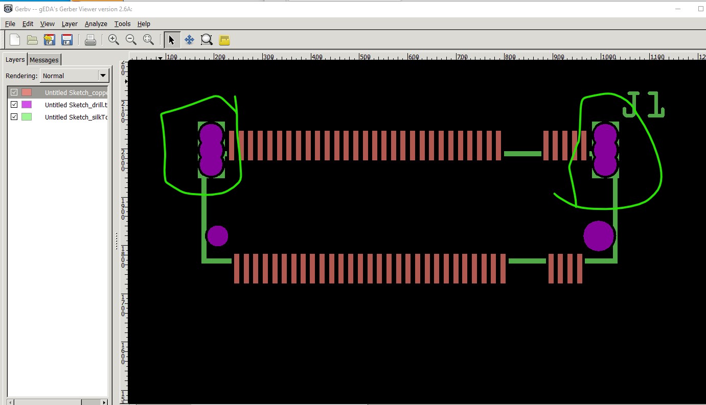
This is the 3hole version and the preferable one if you board house will make it:
attend-123A-85MA0-connector-3hole.fzpz (11.6 KB)
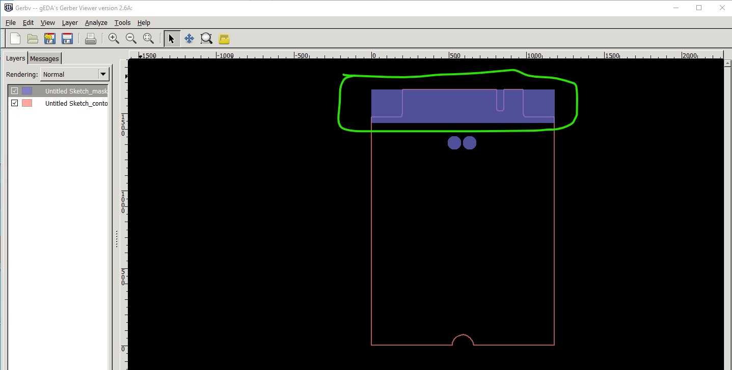
This produces gerbers that look like this:
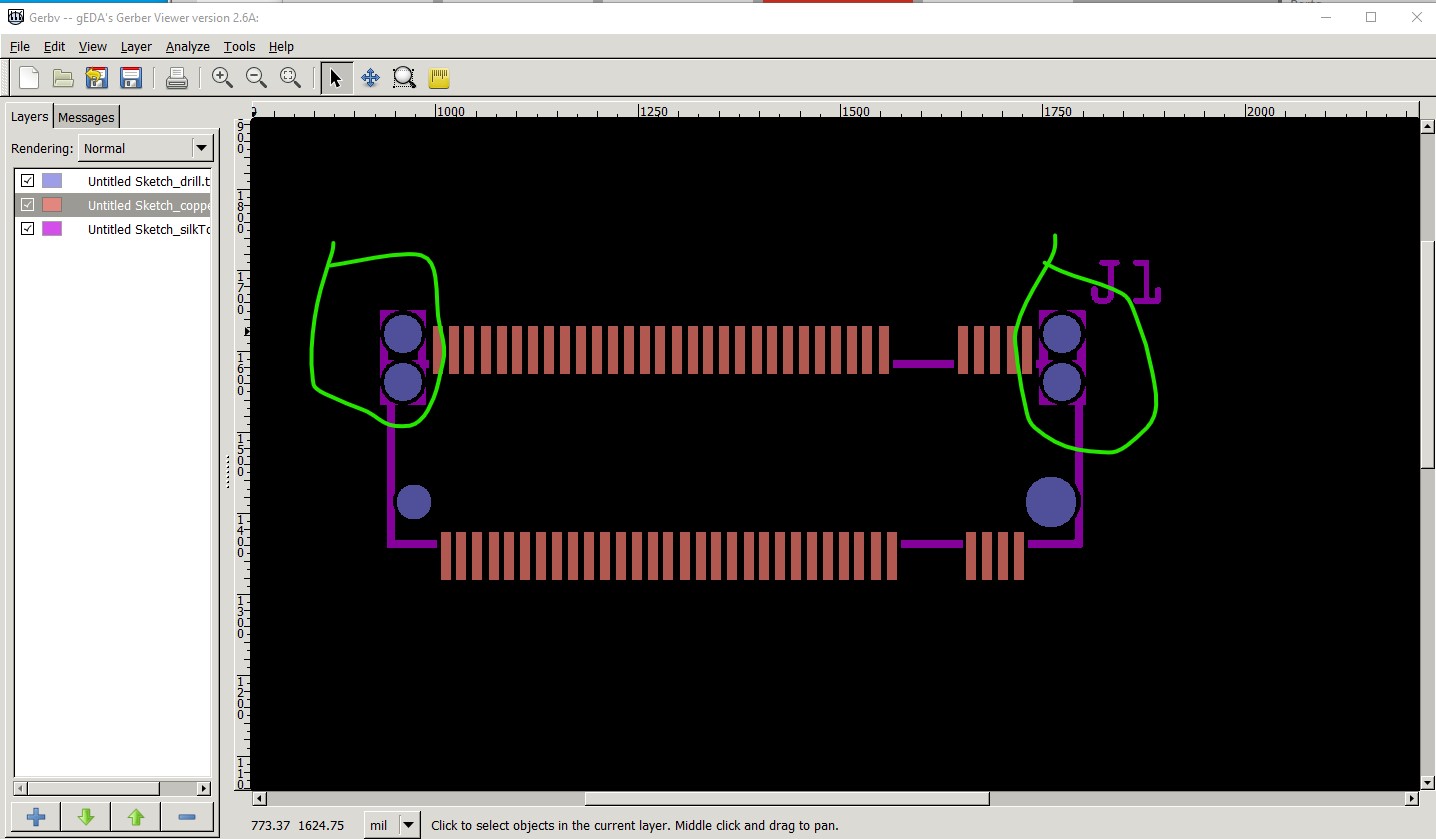
and the two hole fall back
attend-123A-85MA0-connector-2hole.fzpz (11.6 KB)
this produces gerbers that look like this:
which will require more work to make the slots correctly.
Peter