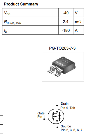
Type
I did not read this
Breakout board, sub assembly, plug in module (A)
Antenna (AE)
Battery (BT)
Capacitor (C)
Diode (D)
Display (DS)
Fuse (F)
Hardware , mounting screws, etc. (H)
Jack, fixed part of a connector pair, header (J)
Relay (K)
Inductor, Coil, Ferrite bead (L)
Loudspeaker, Buzzer (LS)
Motor (M)
Microphone (MK)
Plug, moveable part of a connector pair (P)
[ X ] Transistor (Q)
Resistor (R)
Thermistor (RT)
Varistor (RV)
Switch (S)
Transformer (T)
Integrated Circuit (IC)
Crystal, Oscillator (Y)
Zender diode (Z)
Other (please specifiy)
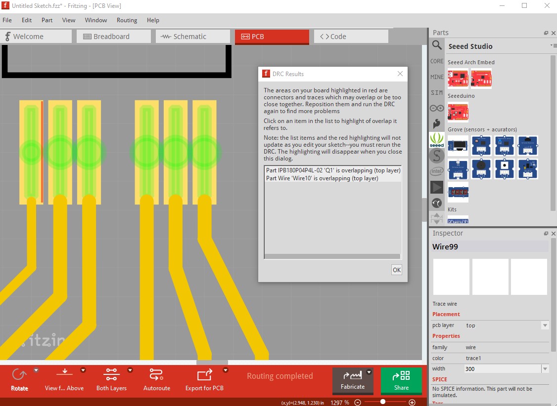
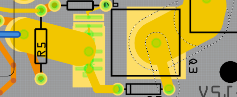
This part should do what you want. Note it doesn’t pass DRC with the default settings so you may need to reduce the DRC rules a bit to make it happy. The gate on pin1 thinks it is too close to the Source on pin2 (which it probably is, but that is what the data sheet calls for!)
as well pin4 doesn’t appear in pcb as it doesn’t actually appear to connect to anything being only a stub. The pad is the only way to connect to the drain.
Thank again Peter, saved my day again. This time I miscalculated the copper of the tab. I had it too small to properly solder the tab.
I don’t worry to much about the DRC. It complains about a solder jumper too. I’m not planning to etch the pcb myself anyhow. Ruined to much in the kitchen and (for me) anything smaller than ‘standard 24mil’ might destroy not only my pcb…
One question arose, I have now several relatively thin wires instead of one extra wide one to connect to the P-fet source. I have (yet) little or none experience with SMD soldering. What I read is that the part more or less aligns itselves (cohesion) onto the centers of the pads. Is this also when soldering with a solder-iron?
What happens if I place one large copper pad under the source pins?
Do i make it myself extra difficult to solder the FET? Or can I better solder a thick (2.5m2+) wire across the source wires? The FET is capable of 180Amps, but I will use a max of 25-40Amp, and I already have a red led in my circuit so I don’t need the glow of my traces to see if the fet is switched on
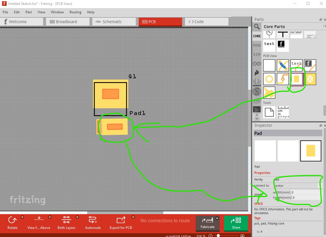
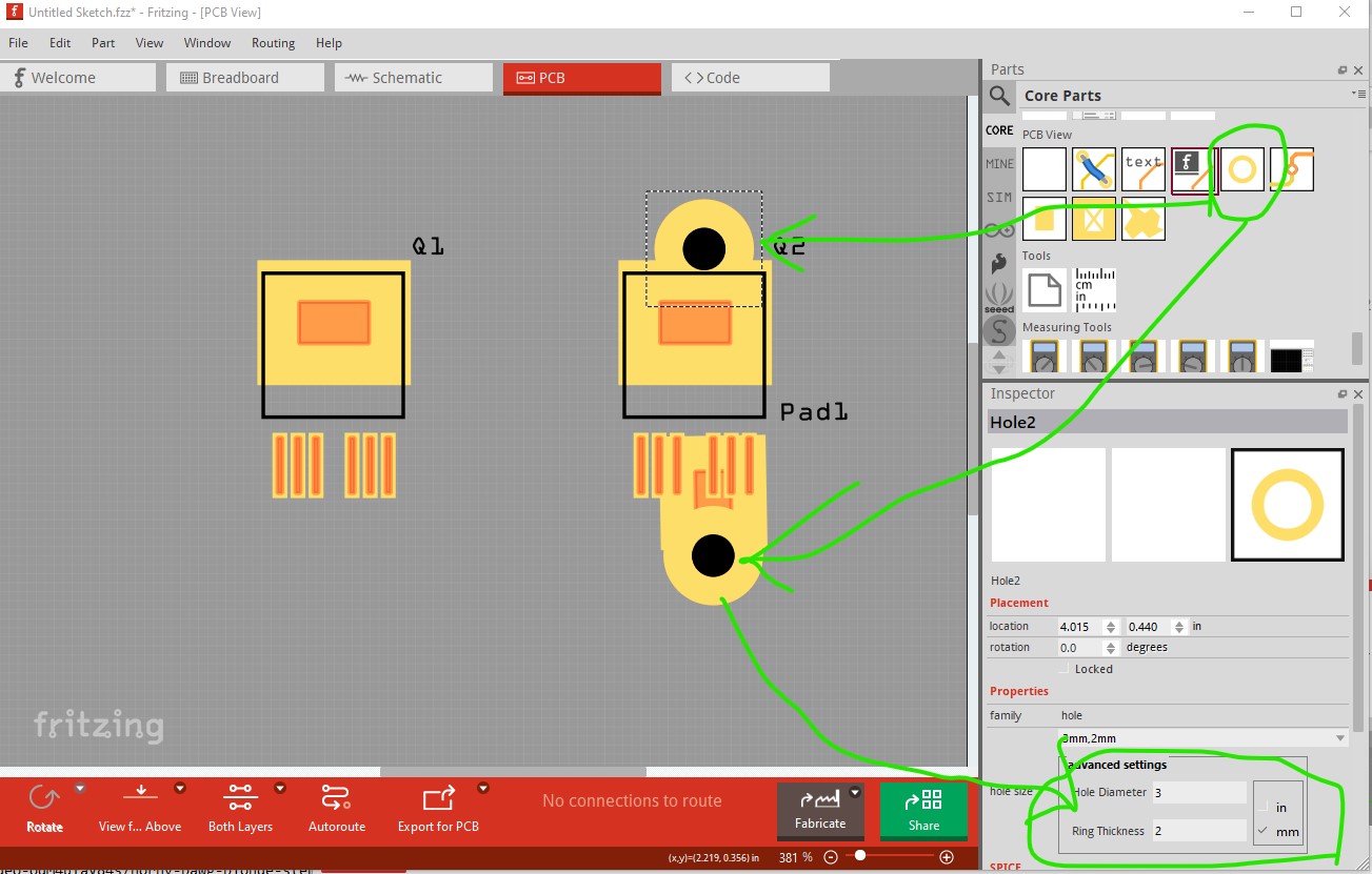
I don’t really know the answer, I have tried hand soldering SMD ICs a couple of times but I find it difficult (old with old eyes somewhat !) I though about a single pad but decided they had recommended a series of them for a reason (which may have to do with wave soldering which is how this is usually done.) If you want to try a pad, drag the pad in to the sketch and put it over the pins like this (you can change the pad size in Inspector)
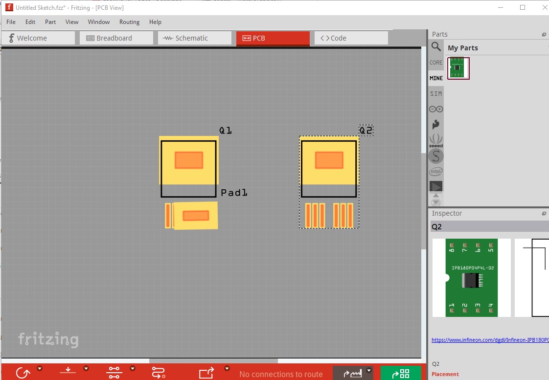
For the price of a test board that should tell you if it works or not. It may be more difficult (because of more copper) to get it hot enough to solder though. DRC will complain about the overlap but it already is anyway. Having both a single part and one with the pad on the same board would be a cheap way of seeing which works better I expect.
You may also need to increase the size of the copper around the drain for heat dissipation (although the RDSSon of the Fet may be low enough to not cause it to heat too much) again not an area I’m expert at. Another possibility is a hole with a large ring area to solder a thick wire into. You can then solder the wire down first and then the FET (I think, although in practice you may need to both at once!) The hole will be through hole and plated so it should support the wire. Mechanical strength is likely to be an issue here, the wire may tear the pads off the board fairly easily. For 40 amps looks like you need about 10ga wire (55A.) You likely also want to specify 2oz copper (as opposed to standard 1oz copper) on the pcb for extra current carrying capacity (but harder soldering due to more copper to heat, always trade offs!) Arranging mechanical strain relief for the wire may also be a good bet to avoid damaging the board. The hole size here is for about 10ga wire which looks to be good for about 55A (8ga for more head room may be better though, depends on how far you need to go!) Looks like the hole on the drain side may need to move up a bit to clear the case though. The black rectangle should be the FET case outline.
Works perfectly!
The pad has a connection too. If you connect that to one of the fet source pins DRC stops complaining about overlap.
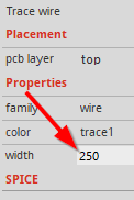
I discovered that you can ‘create’ a custom wire thickness by typing a number over the selected wire width. Here I used 250 mil but you can go as thick as 999mil! I used this before but the drawback for the FET wires was that the wire endings are round and therefore either not connecting all or overlapping others.