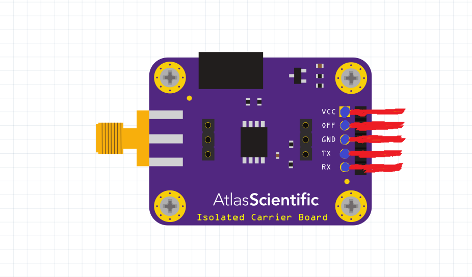
Hello everyone im looking to get this parts PCB view changed. I need the PCB view to have the silkscreen match the carrier broad exactly or slightly larger and can the 5 pins be removed because im planning on using stand offs to attach the PCB to a larger PCB and using male and female headers to connect the pins
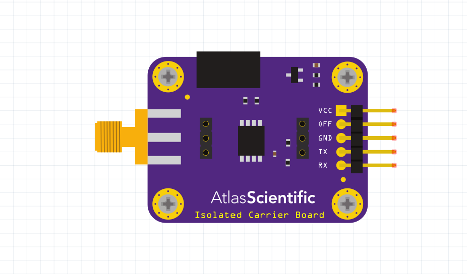
here is the link to atlas scientific page with data sheet:
If all you need is the silkscreen, you do not need a part. Just use an image. In Parts, CORE, PCB view is a “Silkscreen Image” part. Use that and load the image.
This part will do what you requested, but it isn’t clear to me that that is what you want. Without the connectors in pcb there will be no automatic connection to the pins in schematic. If the intent (as is likely) to connect pads on the board via a header and wires to a female header that may be OK, but you will need to connect the header to the part in schematic. In schematic the header is connected to the pins on the part.
This part will automatically drill the mounting holes. Normally I would put them on silkscreen and you would need to drag a hole over them to get the holes, but you likely want the holes without that added step!
edit: Replace with a corrected part (see below for the corrections!)
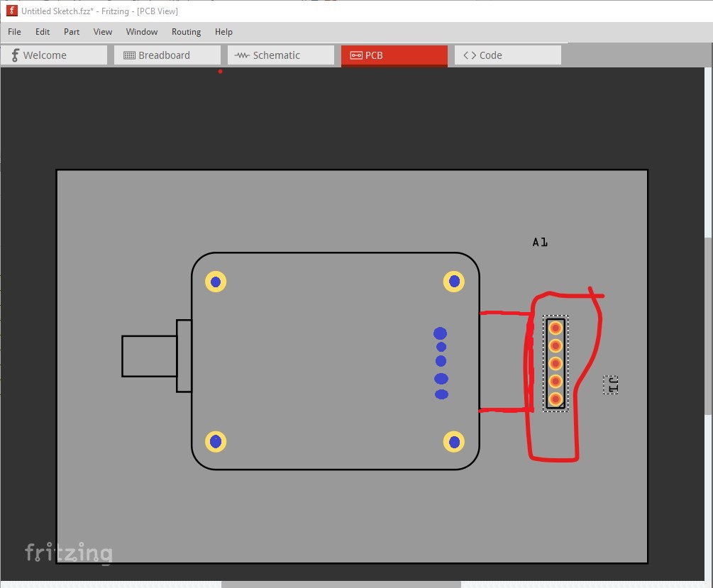
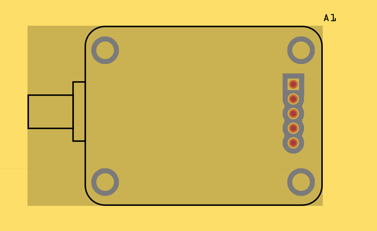
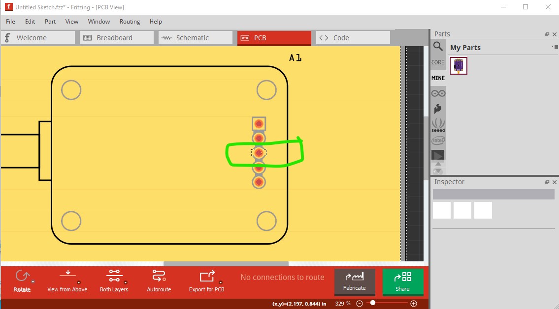
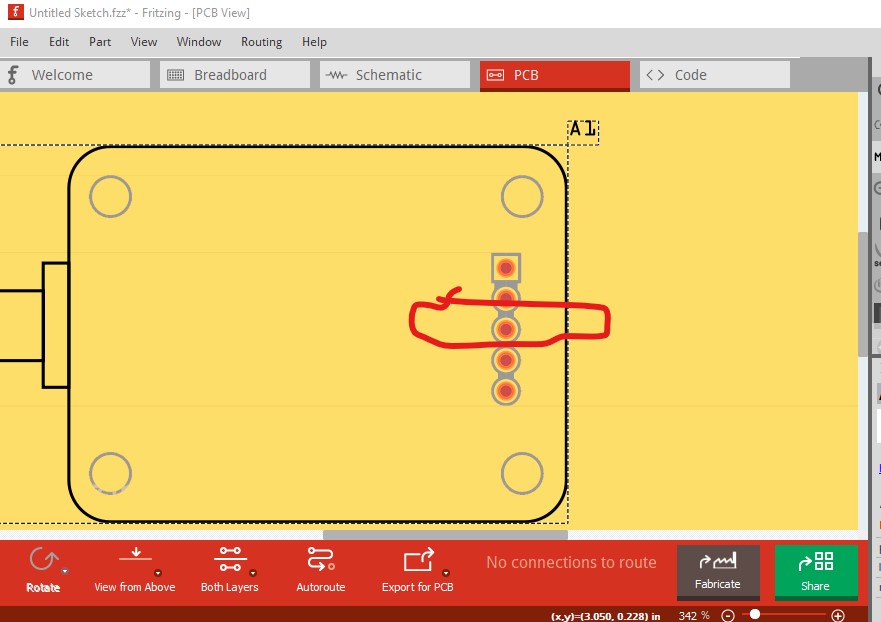
Yes this is really nice thank you but there is 2 things il take a screen shot of your design an use a draw tool to show what i mean (red remove,Blue add). Will the gold circles on the part will they be drilled out on PCB as I will need to use the holes as a mount, as i don’t think i should support the mini PCB with the 5 pins and im sorry I was not clear about removing the connections, I did not think about the Fritzing connections. I meant on this bored I want to DE-solder the male pins that come on the PCB and im going to add male header pins coming off the bottom, then i can “plug” the carrier PCB onto female headers on the main PCB like im doing with the buck converter. also im not sure of the hole location on the carrier PCB but can the silkscreen image be used to get it from or is that not going to be accurate
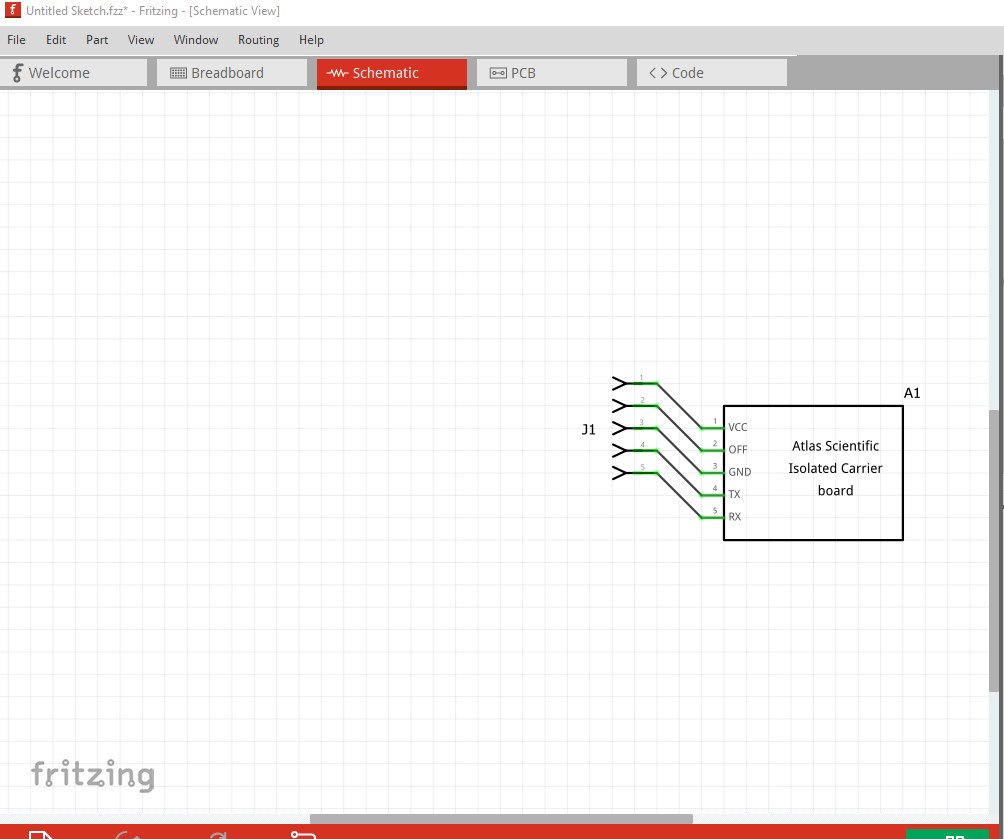
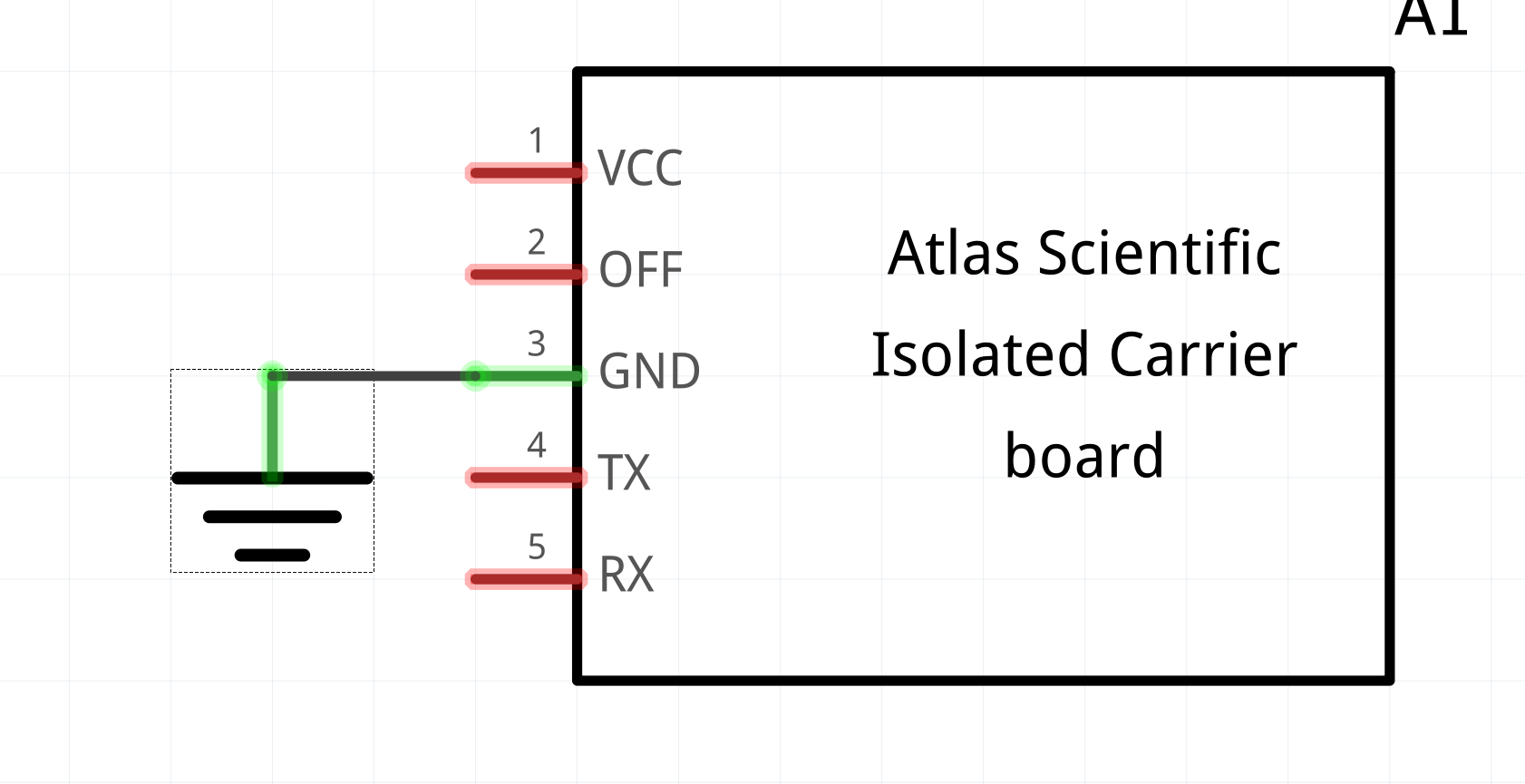
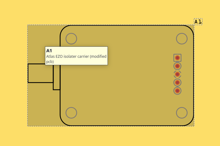
Ah! That makes more sense. The part above has been replaced with a new one that looks like this (J1 is not part of the part, but rather part of the sketch that makes sure the connections are correct!)
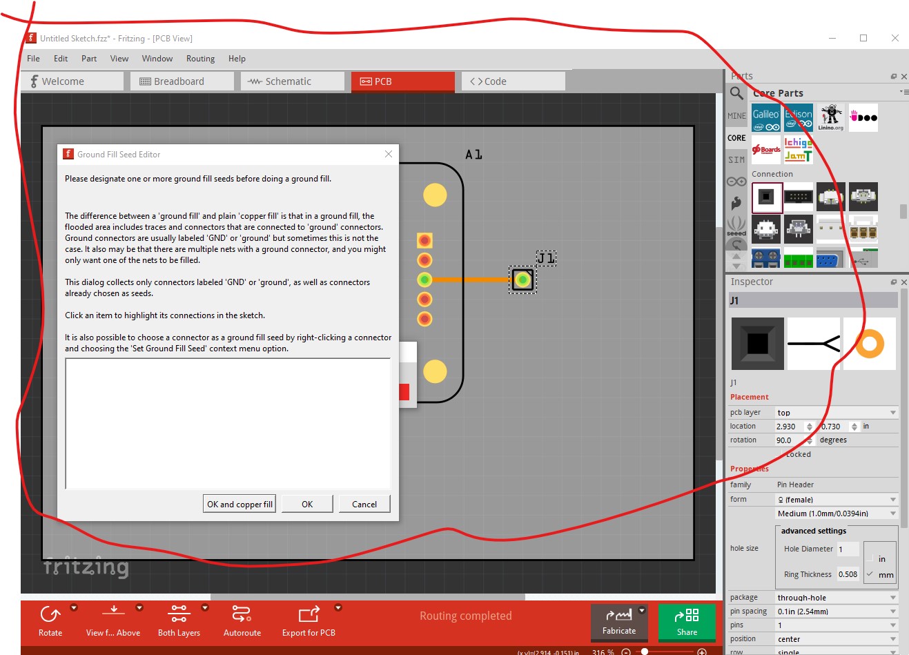
Hey Peter, If you get a chance could you take a peek at the modified carrier broad? It seams like the ground fill wont connect to it. I might be doing something wrong but the ground fill has connected to all my other parts so I made a new sketch with just the board and a ground net and tried filling it and no luck if there is a way to make it link with a trace or something that’s fine.
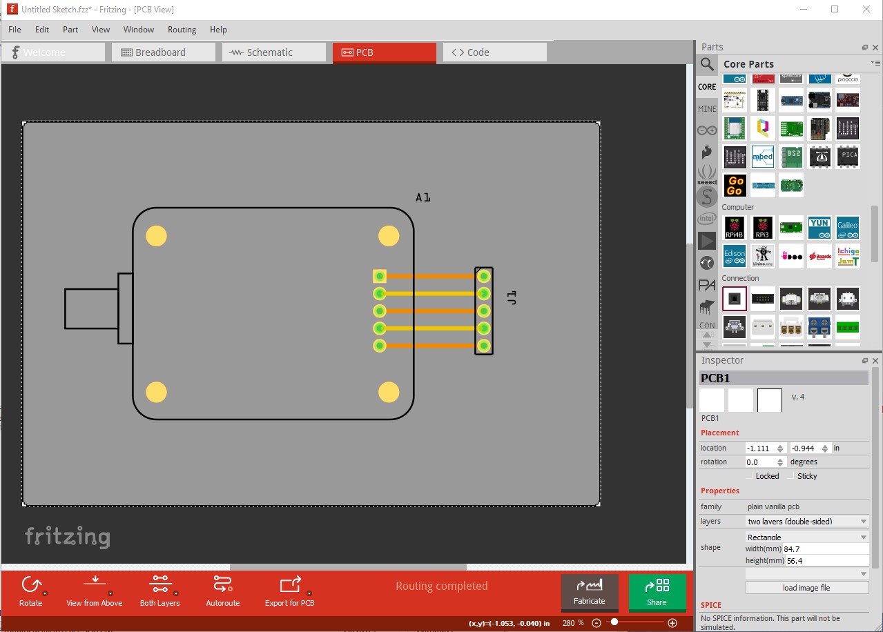
Image:
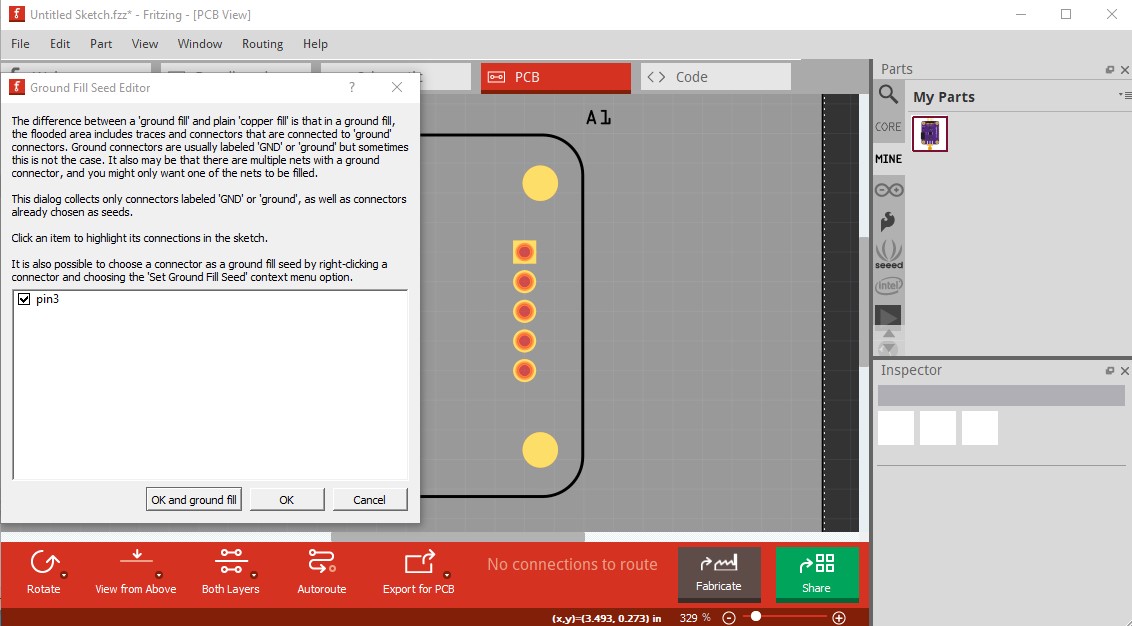
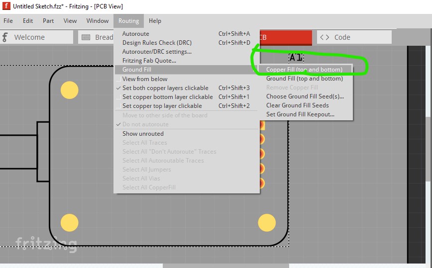
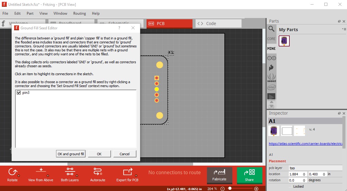
With the reminder this is the first time I have tried ground fill, I can confirm it doesn’t work, but it appears to be a bug (or several bugs.) In Fritzing 0.9.4 (and 0.9.3b) it sort of works sometimes, specifically like this on 0.9.4, here I right clicked on pin3 and clicked “set ground fill seed”. Clicking on ground fill does not work, there is no connection to pin3. Clicking “Routing->ground fill->select ground fill seeds” then clicking “ok and ground fill” does work (which I think is one bug as the normal ground fill should also work!)
Perhaps someone who understands ground fill better than I do (which will be almost anyone ) would have a try with the
Atlas-EZO-isolater-carrier-modified-pcb.fzpz
file above in this thread and see if you can see a problem. The pcb svg in the part is utterly standard (and another part, a 2in fan does the same things.)
edit:
A search for ground fill open tickets on github turns up
which is likely an instance of this. I’ll add a pointer here to the ticket on github.
Ok Thank You for your input, I’m guessing that it would be ok to just run a ground trace from the carrier broad pin, to a separate component ground pin that has successfully linked to ground. this would work as a solution?
Parts editor doesn’t know. You need to edit the pcb svg and look at the diameter which is set to 0.12in (probably from the jpg image and thus may not be correct!) So check a real board for the diameter of the hole, and if it isn’t 0.12in tell me what it should be and I will change it.
I expect Kicad may work, Fritzing (as of 1.0.4) still doesn’t. I just tried the part with a ground fill on 1.0.4 and it still doesn’t connect the ground fill seed to the ground plane (which is a Fritzing bug.)
I made the part (2 years ago now!) for someone that asked for it. My intent was to make a part which I did. There is a bug in Fritzing ground fill that caused some problems (which are still there.) All done as far as I am concerned.
You could try adding a separate ground trace from the carrier board pin to another component’s ground pin, or even check the hole size manually in the part editor to ensure accuracy.
The bug mentioned here is long fixed, since Fritzing 1.0.2.
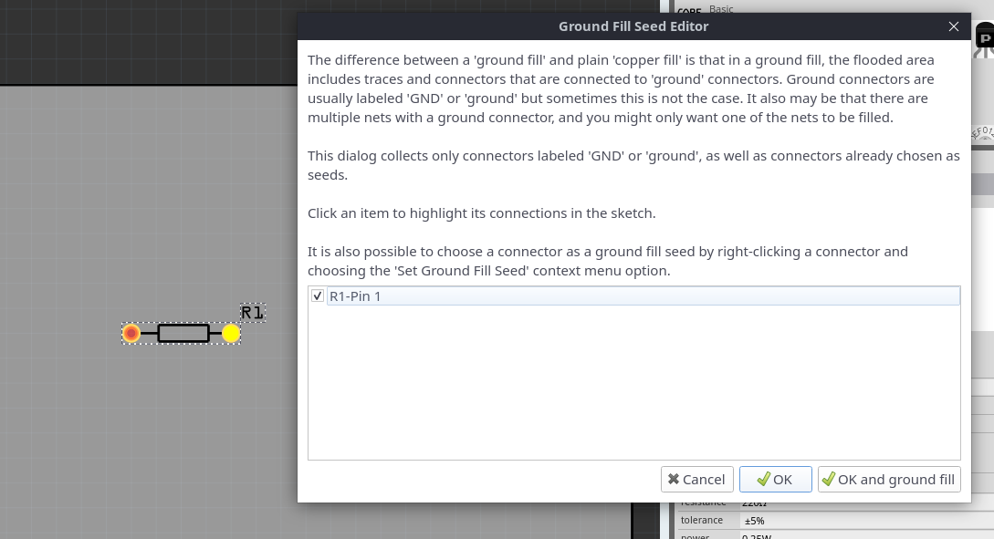
For some reason, probably how the connector is named, although “GND” sounds reasonable,
it is not detected as Ground connector.
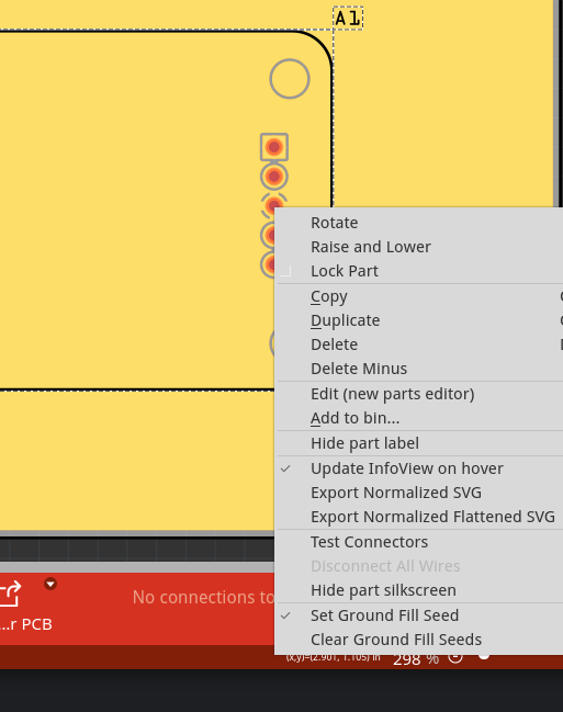
You can manually set it as Ground Fill Seed:
For me on Fritzing 1.0.4 (unless I am doing something wrong which is entirely possible!) it doesn’t automatically set the ground fill nor will it let me set a ground fill seed (which as noted may be operator error!):