Looking for critic with meh circuit

Hi there,

first and foremost: As many posts start with the same phrasing, I’ll pitch into that:
I have virtually no knowledge when it comes to electronics.

Nevertheless, for the past few months I tried to design a robot for no specific purpose other than to fool around.

So I created a Fritzing Schematic for documentation purposes.

I would appreciate any kind of input on the circuit, it is fully functioning as I want it to, I was just wondering where I might improve. I am relatively confident I could get rid of a few wires.

I’d like to create a perforated board for this circuit and thought I might layout that with fritzing and its “auto routing” feature. I invested a few hours to get it look “as good” as it does right now. I just seem to be unable to understand a few routings - f.e. A2 + A3.

Looking forward to any advices / tips on how I might improve. :slight_smile:

1 Like

And for the reason that new users get to upload 1 pic per post, here goes the other one.

A couple quick ones:

It is possible to route this on single side board if you want to etch yourself. (Ordering one made professionally, the cost is not much difference between one and double side though, and you also get the plating in the holes that makes the connections much more robust.)

I would have the big DC-DC converter not soldered board, for mechanical reasons. Instead have matching holes in the board so you can mount in under.

Also for mechanical reasons, I would move the other modules so they are completely over the board.

In prototype and test runs i always throw down some extra pads and connections in a 0,1" matrix for changes/addons/testconnections/whatever.

For circuit analysis, please upload schematic :slight_smile:

It is easiest for us to comment if you upload the sketch file (the .fzz file), that way we can load it in to fritzing and see what is there and make changes and post them.

Peter

MPS.fzz (74.5 KB)

Hi there,

thanks for the input. Attached you can find the .fzz file
Two Parts were downloaded from the web - hope those are attached.

Further information:
I did not change info for the steppers - there are two different I use. Since the actual U/I info does not appear anywhere, I did not bother too much with that.

Concerning the drivers, I modified Vref according to manufacter info.

I did not plan on soldering the DC/DC converter, instead mounting it somewhere as MorganLeij mentioned.

Some modules are not completely over the board for the reason that I plan on mounting those somewhere convenient for the user - f.e. the SD-Card Reader. The circuitboard will very likely be somewhere unconvenient / capsuled.

For any changes you might do, I’d love to get an explanation of why you did do so - so I can learn. :slight_smile:

Anything else?

Thanks again!

Links to stepper-datasheets and the fritzing parts are not attached for the reason I am new and not allowed to post more than 2. If asked for, I’ll provide both in more posts.

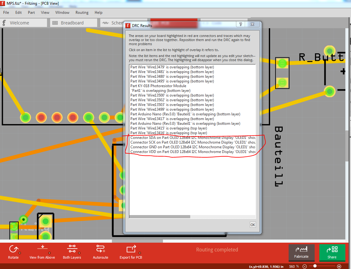
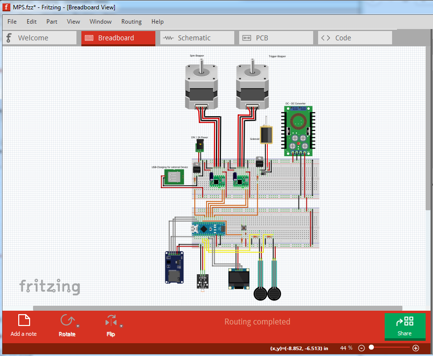
Yes, the folks that designed Fritzing did a good job. When a part that isn’t in core parts appears in a sketch, a copy of the part is included in the sketch so that it will work on any system (which may not have those parts.) That said, one is broken and another ugly so I replaced them. The first thing I did was run DRC (Routing->Design Rules Check) which finds a number of things to complain about:

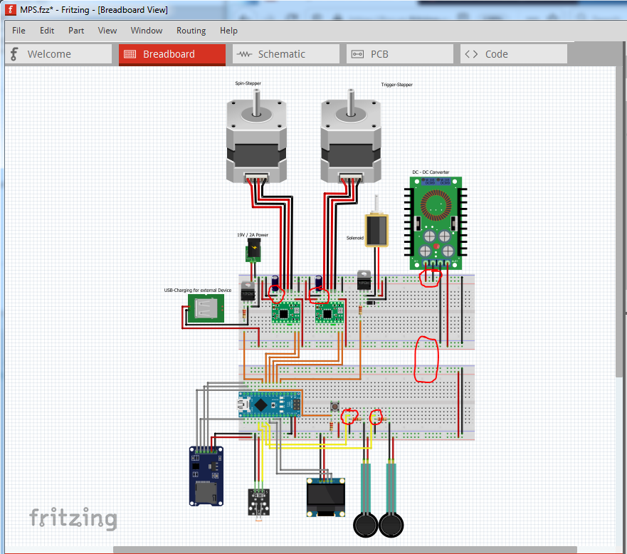
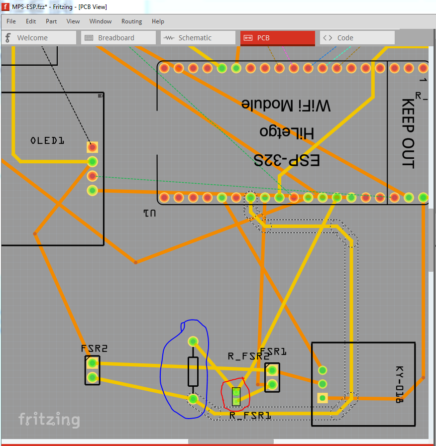
the part circled in red at the bottom indicates that the OLED part is misconfigured (one of the copper layers is incorrectly named.) and you can’t route traces on the bottom layer. The second thing I did was start to route schematic, because breadboard and pcb can look fine but not be fine (and that is true in this case!) That got me looking at breadboard, where there are a number of errors and omissions.

The red circles correspond to these problems:

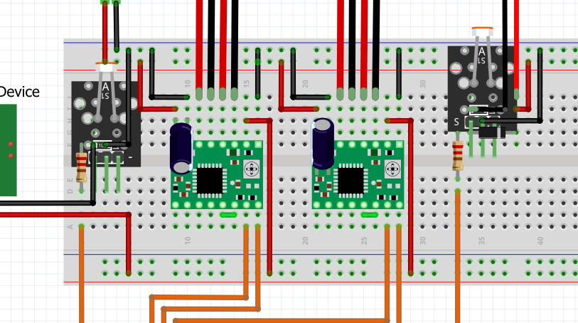
Capacitors are wrong polarity, rotating them 180 degrees to correct the polarity. It is ugly but at the moment the only choice because polarity matters. Moved the motor drivers down one pin to make it a little less ugly.

Move ground on the DC DC converter from positive rail to ground.

move the yellow wire on both FSRs from ground to the other side of the resistor.

move wire from Vin to 5V I don’t believe the Nano will work with 5V on Vin, as there is a 5V regulator in the way I think. It needs to go to the 5V pin but then you need to be careful about plugging USB in as you can damage the USB port. The arduino site has this to say about power:

" Power . The Arduino Nano can be powered via the Mini-B USB connection, 6-20V unregulated external power supply (pin 30), or 5V regulated external power supply (pin 27). The power source is automatically selected to the highest voltage source."

You could put the 19V power in to the Vin pin.

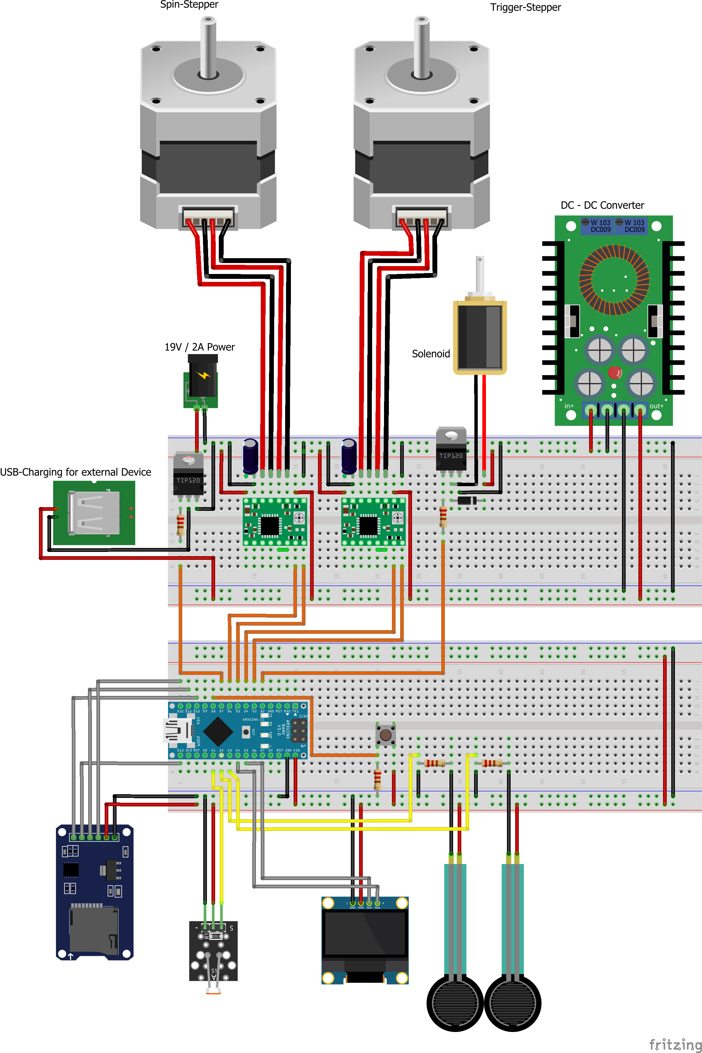
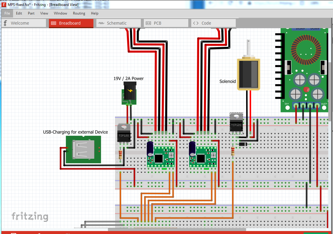
Add +5V and ground connections from top breadboard to bottom to complete the 5V and ground distribution. That gives this corrected breadboard (there is a copy of the sketch later):

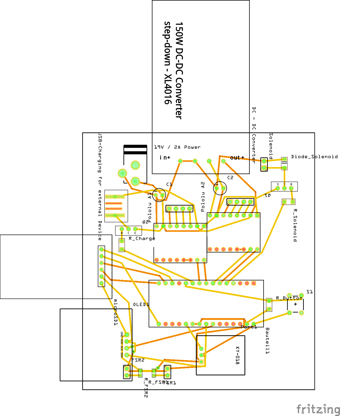
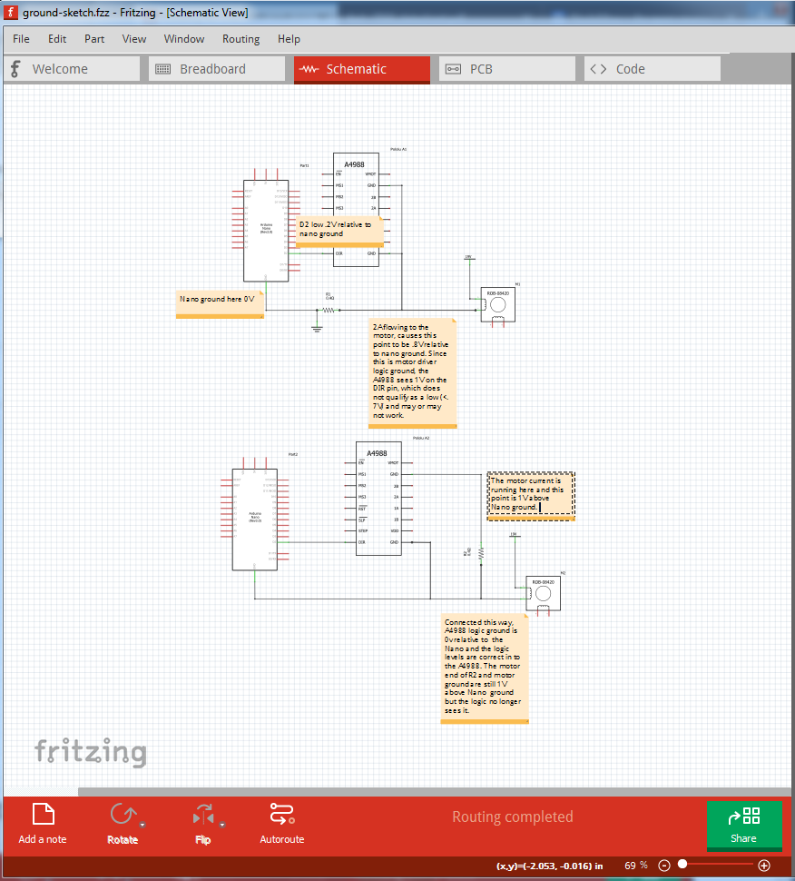
Now on to schematic. Convention in schematic is inputs on the left, outputs on the right, so move the components so the power comes in on the left and the motor and solinoid are on the right. Then arrange things (really done while routing the traces to make schematic readable.) in to a reasonable order. Then route all the traces. I actually did schematic first, it is how I discovered the errors in breadboard. The center of the fsrs didn’t connect to anything, and switching back to breadboard and tracing the wire out from the Nano showed it going to ground instead of the fsr resistor junction where it should. The lack of a +5V / gnd connection between the two breadboards caused a puzzle for a bit. Because I had used net markers, (the upright bar with a voltage, 19V or 5V and the ground symbols) in schematic Fritzing knew the two buses should connect together but there wasn’t such a connection in breadboard. Took me some looking to see where the problem was. A note about parts here. The transistors are overly large, (their scale is too large for the other components and the wire are too large) as well they are not properly postitioned on the .1 in grid so the connectors (for instance ground) connect at an angle. Nothing you can do about this, it is a fault in the part. Eventually it offended me enough that I made a new (better) part and added it. As noted the OLED part is also misconfigured so I replaced that as well.

pcb

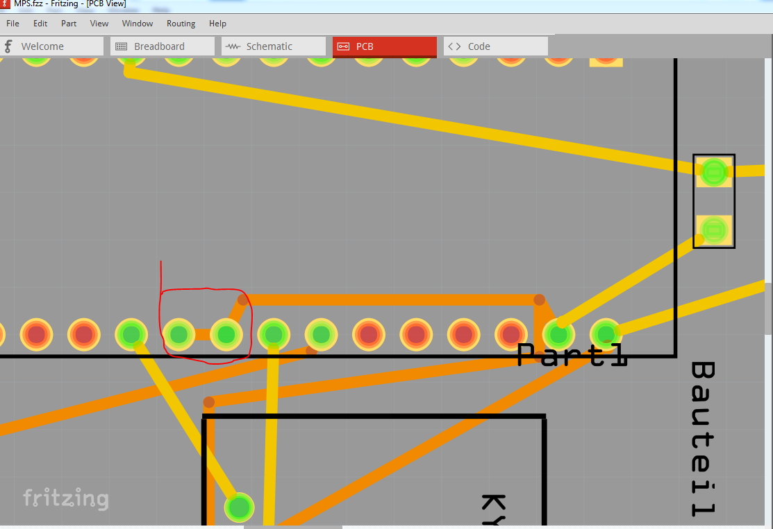
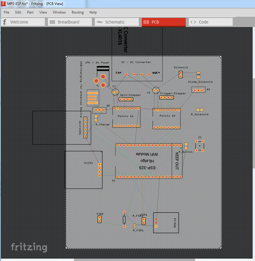
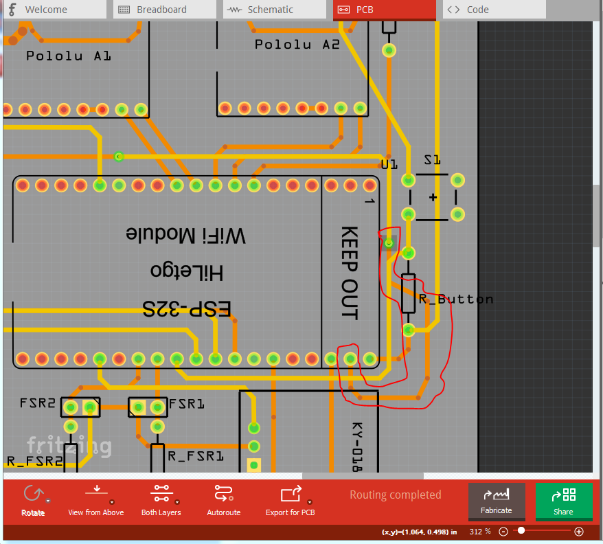
Earlier I had deleted all the traces in pcb (because if breadboard isn’t correct, making changes in pcb is dangerous, as it can cause routing database corruption.) So I was starting from scratch, however loading your original sketch I see another error there is a short between A2 and A3 (which will reflect in to breadboard) circled in red here. The bottom layer trace is shorting A2 to A3

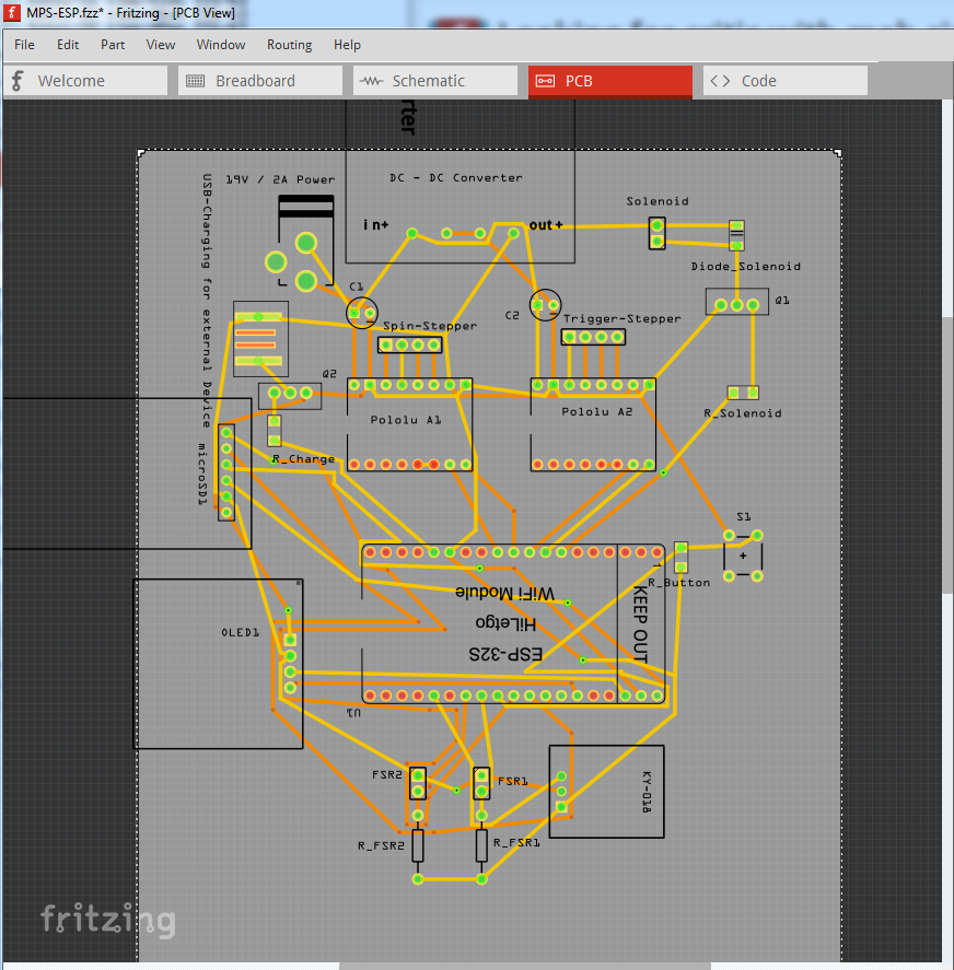
if you click on a pin (try A2 in this case :slight_smile: ), everything else it is connected to will light up yellow. First (as you may know) anything past the boundaries of the grey background won’t appear on the board. So for instance the “150W DC-DC Converter” message will not appear on the board. Then I rotated both capacitors 180 degrees (via right click to select then Rotate 180 degrees) that makes the routing much easier as the traces don’t cross each other. While I haven’t done it, you may want to move the Polulu A2 part right .1in. While I believe (from another board I worked on) they will stack end to end like this, a bit more clearance would be easier. I didn’t move it because there may be a space constraint I don’t know about. I also moved all the labels in to the correct position and orientation (by righ clicking on the label with the part selected and using flip/rotate to change the orientation) so they are all readable. I enabled a couple that were disabled, so if that was intentional you will need to disable them again. Then I did View->Set grid size and changed the default .1 in to 0.05in. This allows me to make 45 degree bends in the traces. Best practice in pcb design is considered be to have all traces vertical or horizontal and connections betweem vertical or horizontal segments at 45 degrees (no 90 degree bends.) This is mostly important at RF and for EMI suppression, but it is a good habit to learn even when not doing RF or worrying about EMI. Then for the Vmot connections and grounds, because they are high current, I selected the trace then in Inspector (the lower right window) set the track size from the default 24mil to 48mil for all the high current paths (including the external USB charger ground.) Now all the digital grounds should connect together and then connect once to one of the high current ground points. The reason for doing this is the high current grounds will exhibit a slight change in voltage due to the high current flowing in them which may have an undesirable effect on the logic circuits (this is why there is a digital ground and a motor ground on the motor driver chip.) At this point I fixed up the Tip120 and OLED parts and used delete minus to replace them. Delete minus deletes the selected part but leaves the traces that connect to it, so you can load an updated part then (in all views) click on the end of a trace and move it off and back on to the pin of the new part until the connection goes from red (no connection) to green (connected.) The end result of all of this is this sketch (which you need to check to make sure I didn’t make any mistakes :slight_smile: .)

MPS-fixed.fzz (107.2 KB)

This sketch has the following two parts in the temp parts bin, but I will include them here for anyone later searching for corrected versions of these parts:

OLED-128x64-I2C-Monochrome-Display-fixed.fzpz (9.0 KB)

TIP120-Hi-Current-Darlington-Transistor-fixed.fzpz (6.4 KB)

Peter

Hi Peter,

… Wow.

I’ll dig into your reply, which will def. take me some time.

I am taken back by the amount of time you invested. May I ask how long your corrections took you?

Some few quick responses:
19V on VIN did not work out nicely - burned a few arduinos that way, which made me hook it up to 5V. Due to the USB-Charger, the DC/DC Converter is needed, so that change did not hurt.

And for some reason I did not look into yet, exchanging the TIPs did not work out perfectly, check attached image. I will let you know as soon as I figured why it looks the way it does.

Thanks again for your wholesome effort! :slight_smile:

I am fortunate enough to be retired (11 years in February) so my time is my own to do what I like with. I have 50+ years of help from smart co workers to pay forward to the new generation of folks coming after us. The changes took me a couple of hours, most of that in fixing the parts. I am familiar enough with what goes wrong in sketches that fixing them up doesn’t take that long.

19V is on the high end of the acceptable range, a resistor in series to drop the voltage would probably help, but if you need the DC DC converter any way, regulated 5V is better. However I’d expect applying it to Vin wouldn’t work as there is a 5V regulator (which needs about 7V to operate) in the way I think. As noted with 5V applied you need to be careful with the USB connection, because as I recall there is no diode protection for the USB port and it is possible to damage the host USB port if it is has a bit less than 5V output. Computer USB ports are much more expensive than Arduinos :slight_smile: .

That is odd! It looks like it is picking up a different part rather than the tip which might be my fault if I screwed up and duplicated a moduleId, but there should be a complaint if so. For me they seem to work fine. Try loading the sketch I uploaded and see if it does the same thing (that is what this image is from.)

Peter

Hi there,

I invested a few hours aaand …

Changed to a ESP32 due to memory-shortage with the nano. I am sure I will have to redo the whole fritzing-file but started with modifying yours for practice.

Unfortunately the breadboard view looks horrible, I think.

1.) I was unaware of the 5V/VIN problematic. Thanks for pointing this out.

2.) The tip with the yellow dots makes everything so much easier. Of course I saw them lighting up but chose to ignore those with the first go. This time, I enjoyed using them a lot.

3.) You are right with the moduleID. I went with deleting all “MINE” parts and woosh - everything was looking nicely.

4.) I started with the breadboard-view for the ESP exchange, again, I dont like it too much. The physical version looks a bit different because I went with a “smaller” ESP part with fritzing. Makes it possible to use only one breadboard instead of two like I do in the real world. Another reason why I will redo the whole fritzing thing but again - I did not want to delete all your work and start from stratch straight away.
I invested lots of time in the schematic view, which looks not too bad, I think. Two questions arose while doing so:
How hard would I try to avoid crossing lines? You did a few times, I simply went nuts avoiding crossings. This is why my schematic looks weird, I think.
Is it a convention to have Voltage facing upwards and GND facing downwards? I figured that with your work and then went the same way.

5.) I listened to your hint and connected logic-gnd of the drivers to logic gnd - I dont understand it though. GNDs are all connected, so why would this make a difference?

6.) PCB seems to be a whole different level. I’d guess this is what typically takes longest to create. I will dig into that and post results - but another day.
Would it be a helpful to arrange the parts similar to schematic and start routing from there? Are there other conventions besides the 45° bend?
I will start connecting grounds as you mentioned and … see where I am going to end up. :stuck_out_tongue:

Thanks so much for your help!

MPS-ESP.fzz (116.3 KB)

If you don’t need the wireless, another option is a blue pill. That is a Nano sized board with a 32bit Arm cortex cpu running at 72mhz (so much faster) and with 128K of flash and 20K of ram (but no wireless, and no lua (which I believe along with the wireless eats a fair amount of the extra flash and ram in the node mcus.) The blue pill can be programmed from the Arduino IDE. That said, if the node mcu has enough flash and ram for what you want to do, then it is a good solution too.

As long as you are careful and start by doing routing-> select all traces delete in schematic and pcb and then complete breadboard, you should be fine. Making changes in more than one view can cause problems if you make mistakes. Something corrupts the routing database (I have 3 or 4 examples but so far can not recreate the failure by undoing the changes and redoing them to try and fix it.) Once breadboard is complete, then connect and route the rats nest lines in schematic and pcb.

There is a node mcu with the 1.1in spacing (which it sounds like you have) in the forums somewhere. I have made 5 or 6 versions of this for all the different boards folks have come across. Breadboard looks fine to me, although it is desirable that it match the real world for documentation purposes.

they are especially useful when routing pcb. The rats nest lines connect to the closest connection on the same net. By clicking on a pin you can see all the possible connection points and possibly find a less obstructed path to make the same connection.

I agree it looks great! The SD card power pins being misaligned to the grid (not your fault, the part is broken) is annoying but other wise it is very clear. That is the objective, making a schematic that is easy to read. Sometimes you can’t avoid crossing lines, but try and avoid it as much as possible.

Yes, usually power is on the top and ground on the bottom in schematic.

While we normally assume a wire is perfect with no resistance, in the real world that isn’t true, wires (and traces) have resistance (not much but some.) With logic the current is low 10s of milliamps and ground is ground works in practice. When dealing with motors, and solinoids or anything that draws a lot of current, the wire resistance starts to matter. If a trace is carrying 2Amps and has a resistance of .4 ohms there will be a .8V difference in voltage from one end of the wire to the other. The logic circuits consider a low to be between 0 and .7V and a high to be (usually) 2.4V to VCC (3.3V or 5V). A signal between .7V and 2.4V is neither high nor low and will cause problems. Here is a schematic that shows this

Since I’m not sure how readable this will be here is the sketch as well (where you can zoom in to read better):

ground-sketch.fzz (8.3 KB)

The .4 ohm “resistor” is really the trace between the motor ground pin on the A4988 and the motor with its internal resistance.

I was poking at your new layout’s pcb for a bit, and have some suggestions. Assuming you don’t need SMD resistors for some reason I’d switch to through hole. That gives you more room to run traces between the resistor pins which will make routing easier. Changing the smd (circled in red) to tht (circled in blue) gives you a bunch more room to route traces and allows traces on both sides of the board which makes routing easier.

As well I’d probably start here (with all the traces deleted) and then move the components around (if there isn’t a reason they need to be where they are) to make routing easier.

for instance I’d move the motor drivers so they are at the same level unless they need to be where they are for some reason, and try and make the board as small as possible (because part of the board cost is the number of square inches so smaller is somewhat cheaper.)

Then it becomes route the traces, then use click on pin to highlight connections and see if there is a better route to another connection, when routing gets difficult see if moving components around will make it easier. It is trial and error (and gets easier with experience) to get acceptable routing. You can also try autorouting, but it typically doesn’t work that while (because this is a hard problem) and either won’t complete or makes a very messy layout, but it can be a place to start. Autoroute did complete (somewhat to my surprise) but the result is pretty ugly and can be made much better I expect. DRC (routing->design rules check) is pretty unhappy about the clearances, but that is probably fixable.

This may not be a bad place to start from and try and remove some of the uglier traces.

Peter

So, I went back into it and am relatively satisfied with the PCB layout. The microSD module I connected last. This might be the reason for a view Vias…
Next time, I’ll start with the breadboard, go to schematic and then “copy” the layout to the pcb - that should make things easier, I think.

I followed your advice and this is the result:

This is my .fzz file.
MPS-ESP.fzz (126.4 KB)

So far, I learned a lot. Thanks Peter for the time you invested in this post.

I’ll start working on the new file this week and will post the updates aswell.

Again, thank you Peter! :slight_smile:

Best regards,
Sam

Looks great! The one change I would make is to reroute one trace so it is out of the keepout area on the wireless module. They don’t want any copper in the keepout area as it affects the antenna for the wireless (at least potentially) and in this case it is easy to avoid:

MPS-ESP-improved.fzz (126.7 KB)

Peter