This is a great actuator motor controller and seems quite popular. I want to document my project and beforei embark on creating this part I was wondering if anyonehas made or come across this part. My initial half day hunt has not signed anything up.
Any update for this part?
I tried to make my own part, but I failed to import the fonts and printed view from Inkscape.
I’m a beginner to creating components on Fritzing and my comprehension of svg/xml files is very limited.
Even with the usage of Vanapp script, the SVG file didn’t import it correctly.
I share my SVG files if someone has the patience to make a proper one.
jrk-g2-21v3-fritzing.zip.fzp (253.2 KB) (Don’t forget to remove the .fzp extension)
I will be deeply grateful to him ![]() .
.
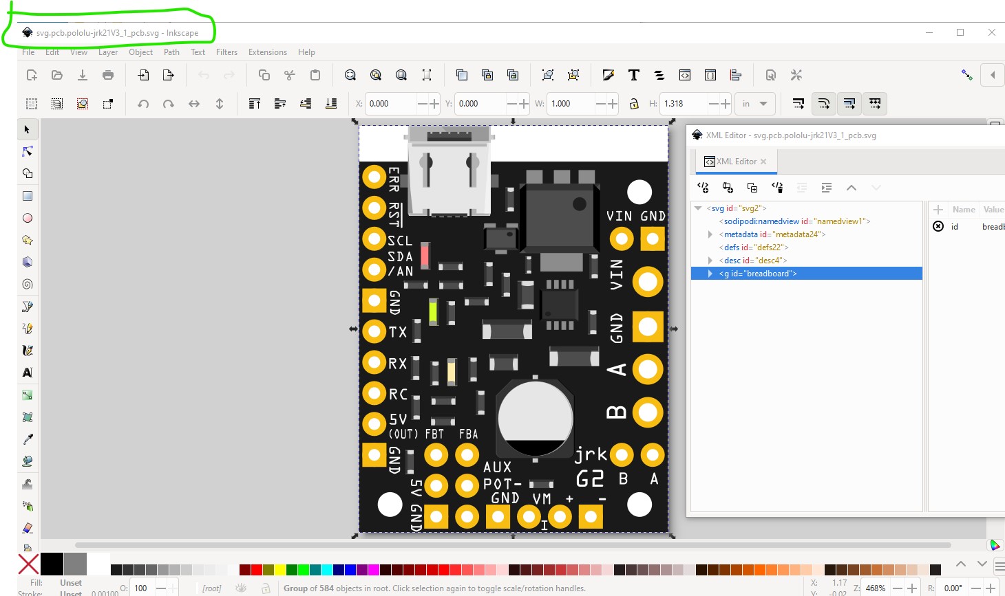
This part should do what you want.
pololu-jrk21V3.fzpz (19.9 KB)
note the mounting holes are not drilled by default. If you want mounting holes in your sketch you need to drag in the core parts pcb hole item and set the size appropriately. Here is how I made this part (unzipping the .fzpz file will get you the .fzp and svg files referenced below.)
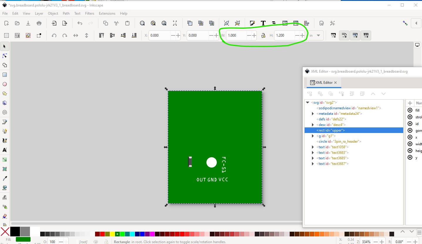
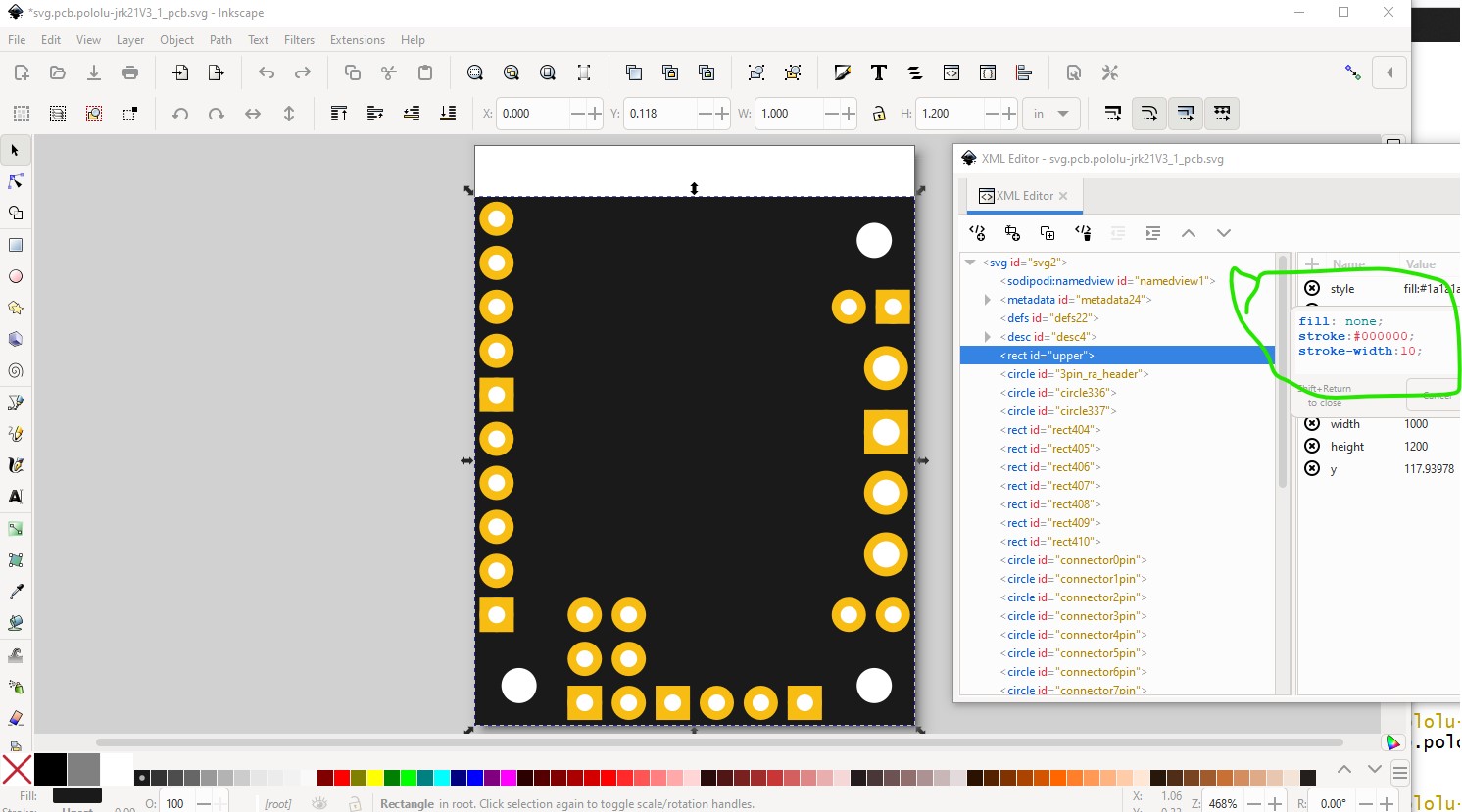
Start with a standard template then set the board to the correct size (from the data sheet)
import a jpeg image of the board then scale it (by locking width to height and then changing the width til the jpg matches the board size)
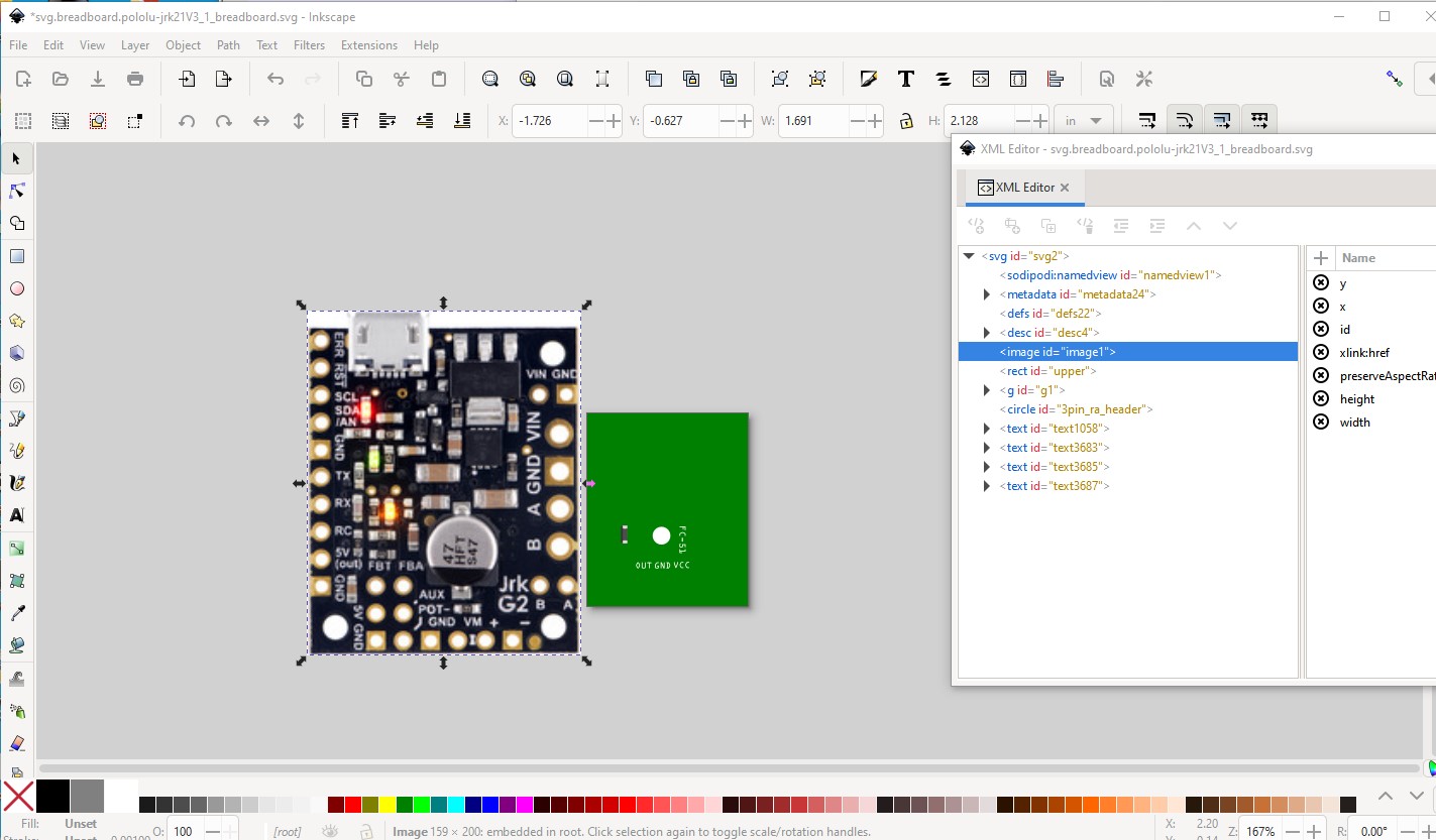
then move the board to the back to uncover the image (leaving the board aligned with the jpeg image.)
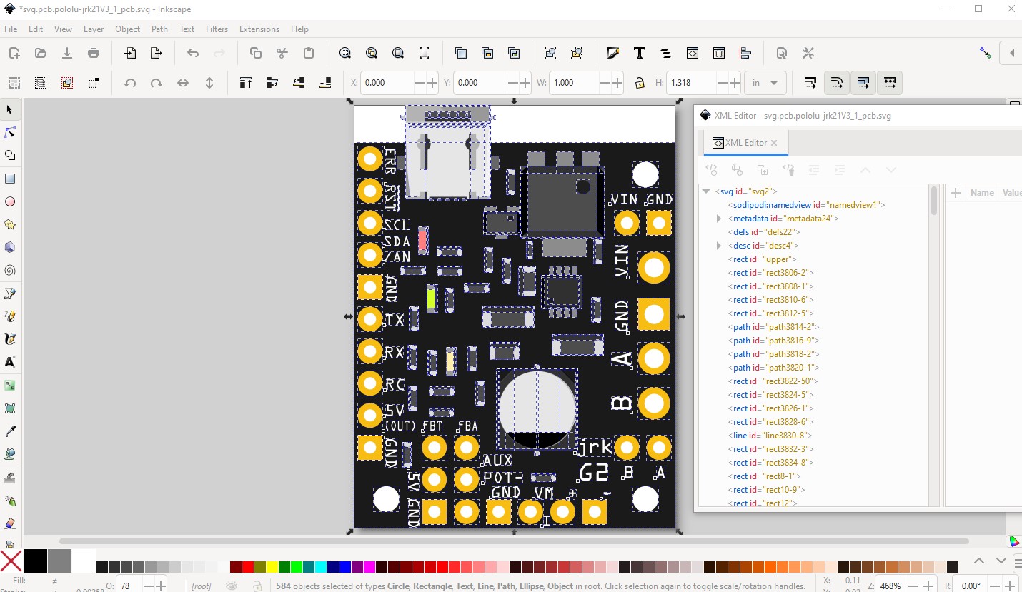
copy in breadboard images for the components
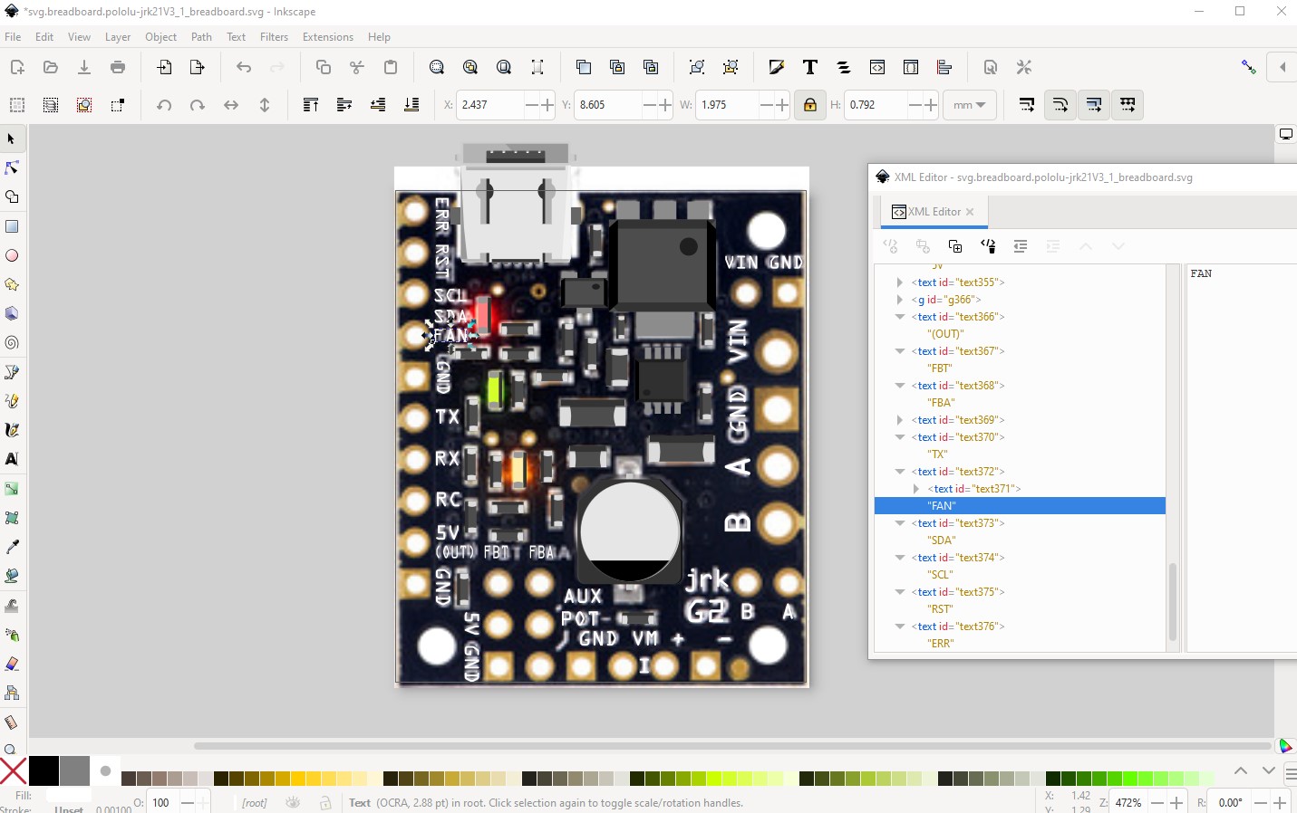
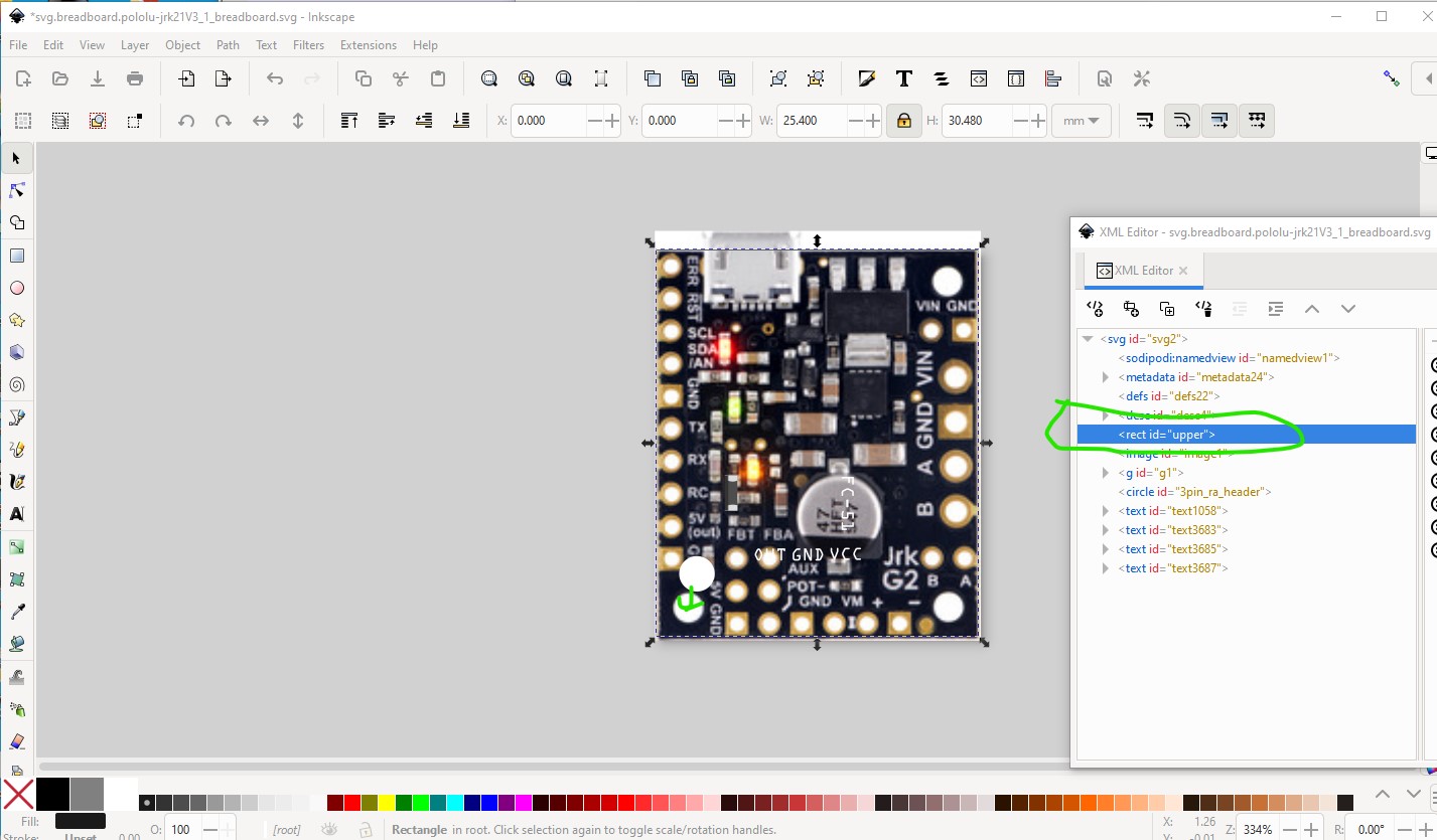
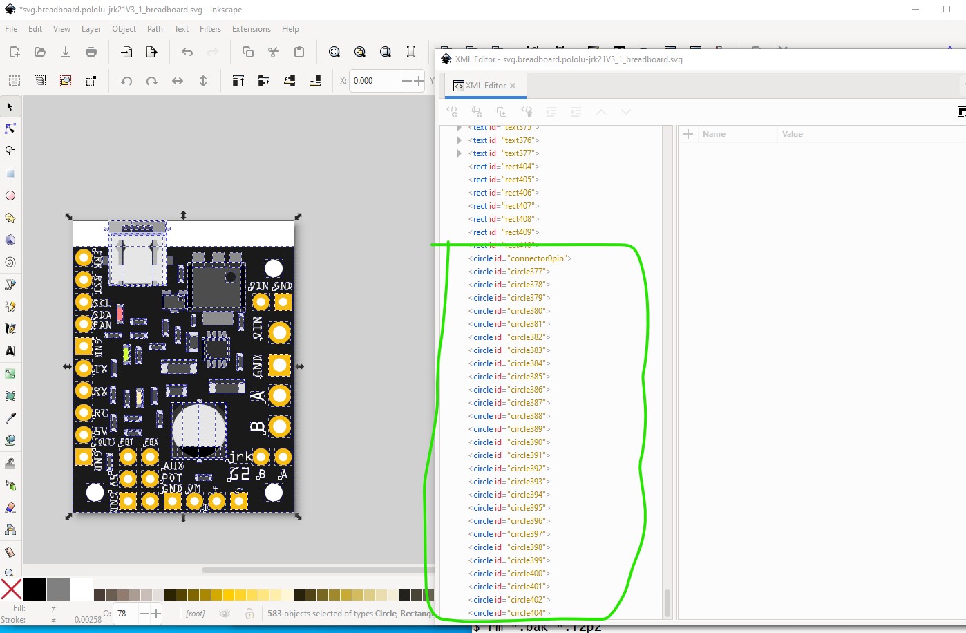
for everything except the connectors (the red circles.) here the image is in the background so the breadboard view appears.
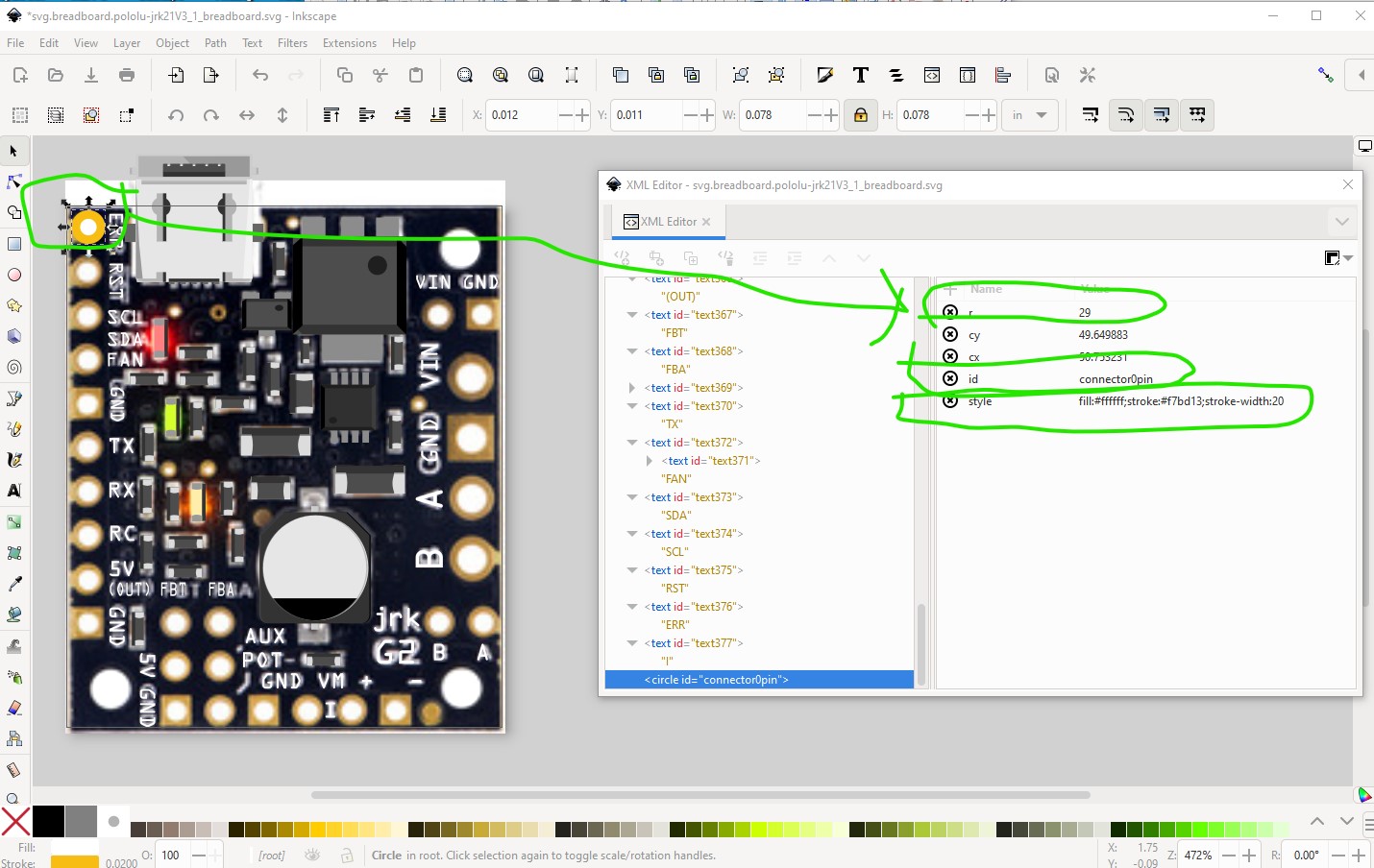
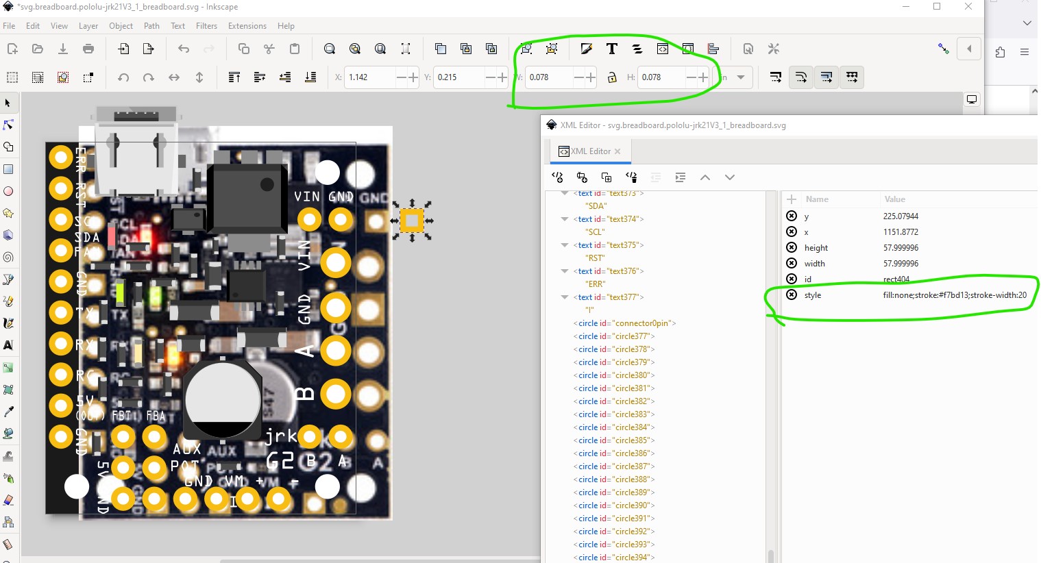
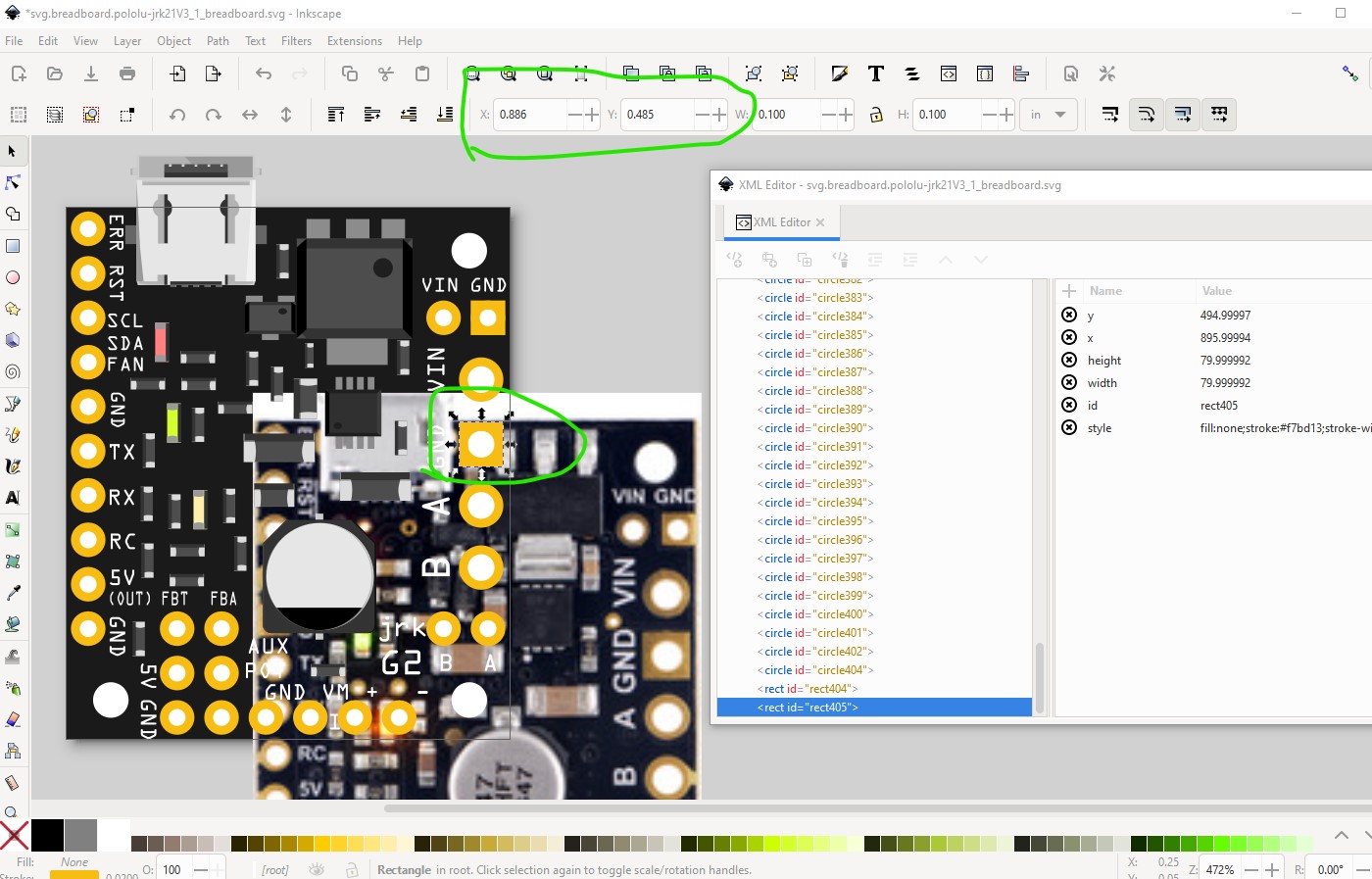
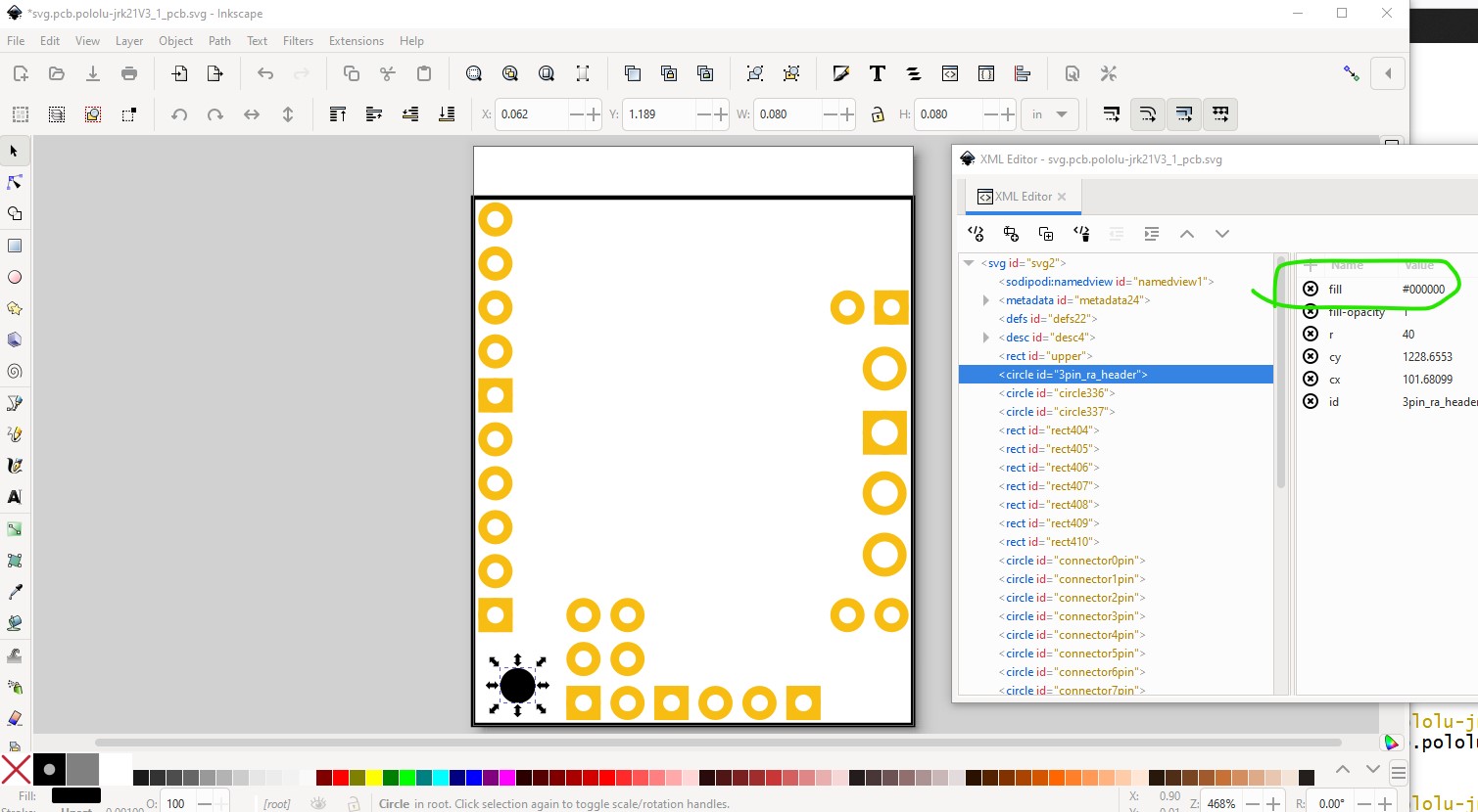
Create a circle (set to be a 0.1in header pad) for the first connector. Set its id to connector0pin.
duplicate it and move it down 0.1in with the tool bar
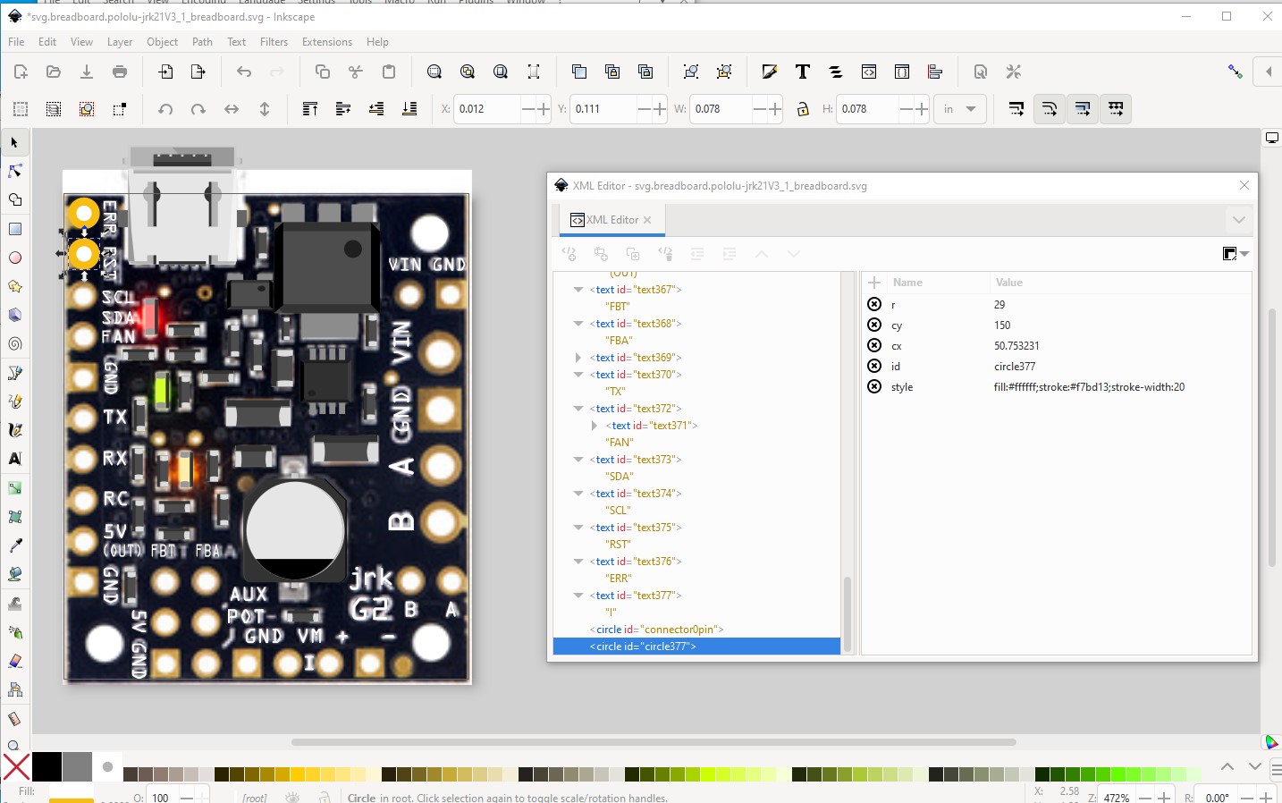
rinse and repeat for the rest of the connectors in order
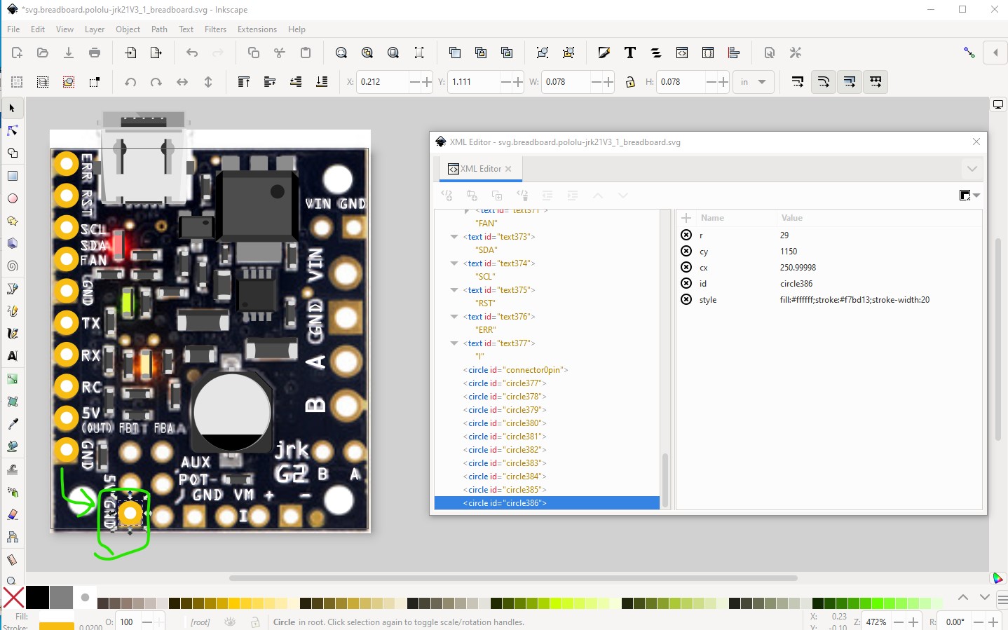
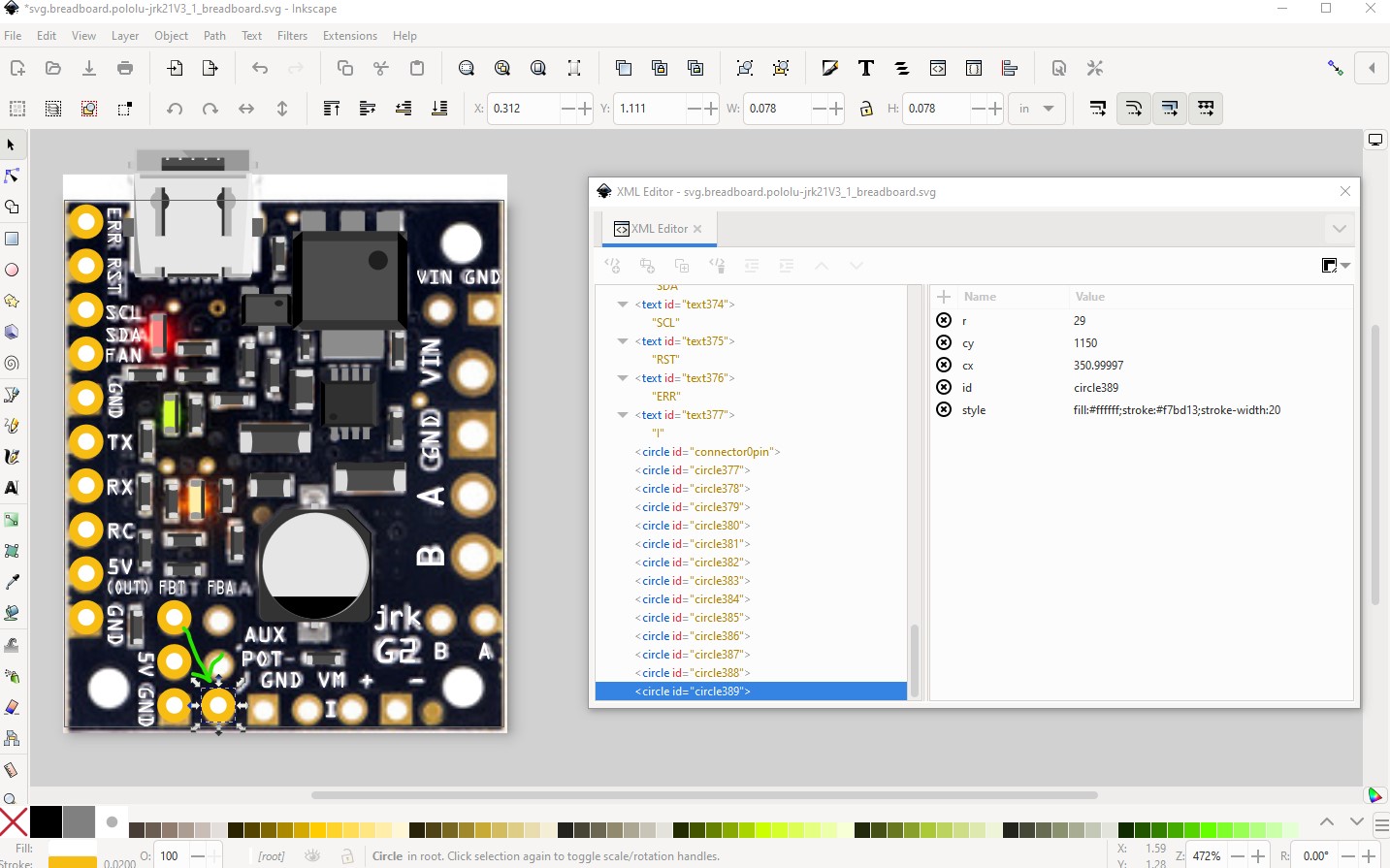
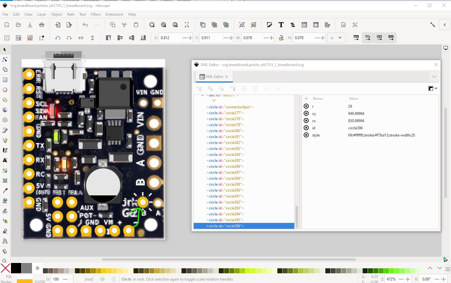
at this point increase the radius of the pad to make it suitable for the screw terminals
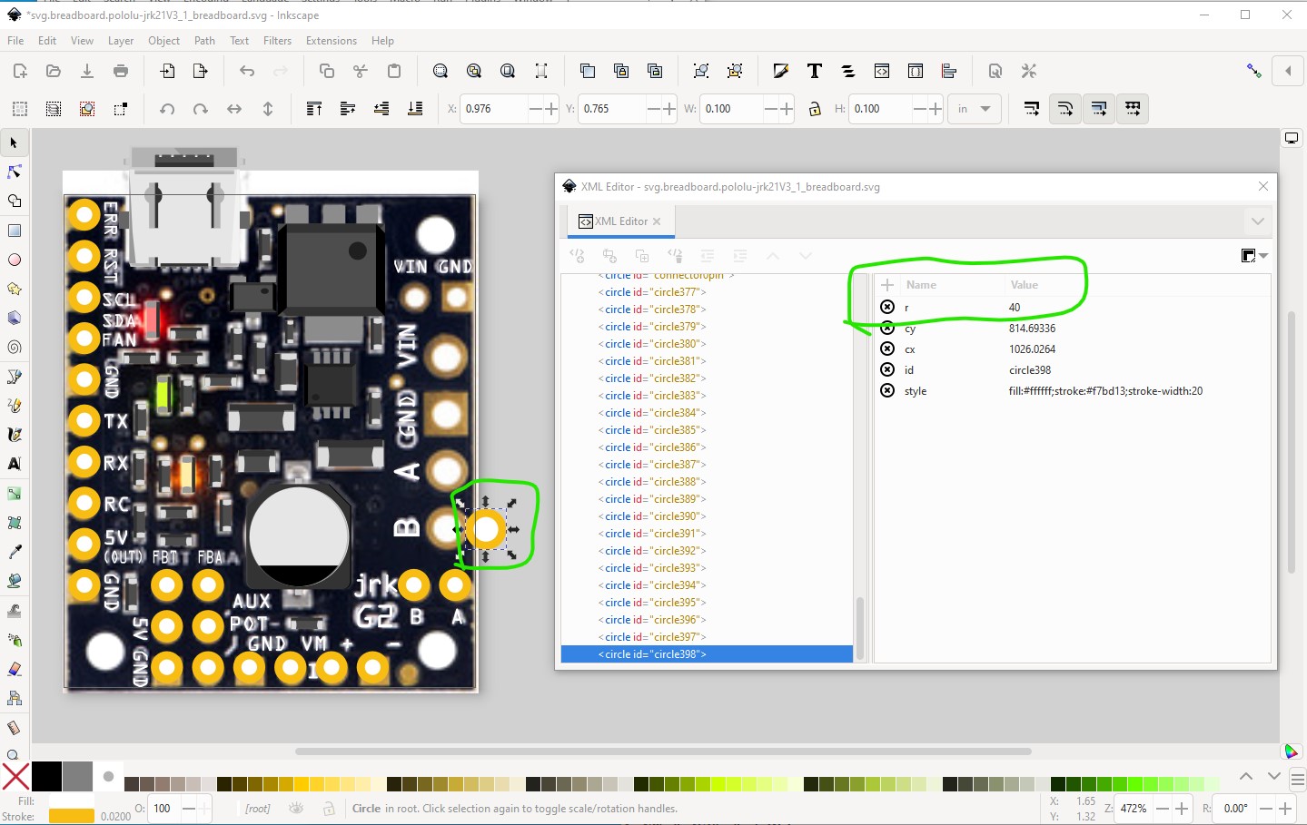
then dup a 0.1in header again for the top connectors
that produces all the connectors in the correct order with the first one marked connector0pin.
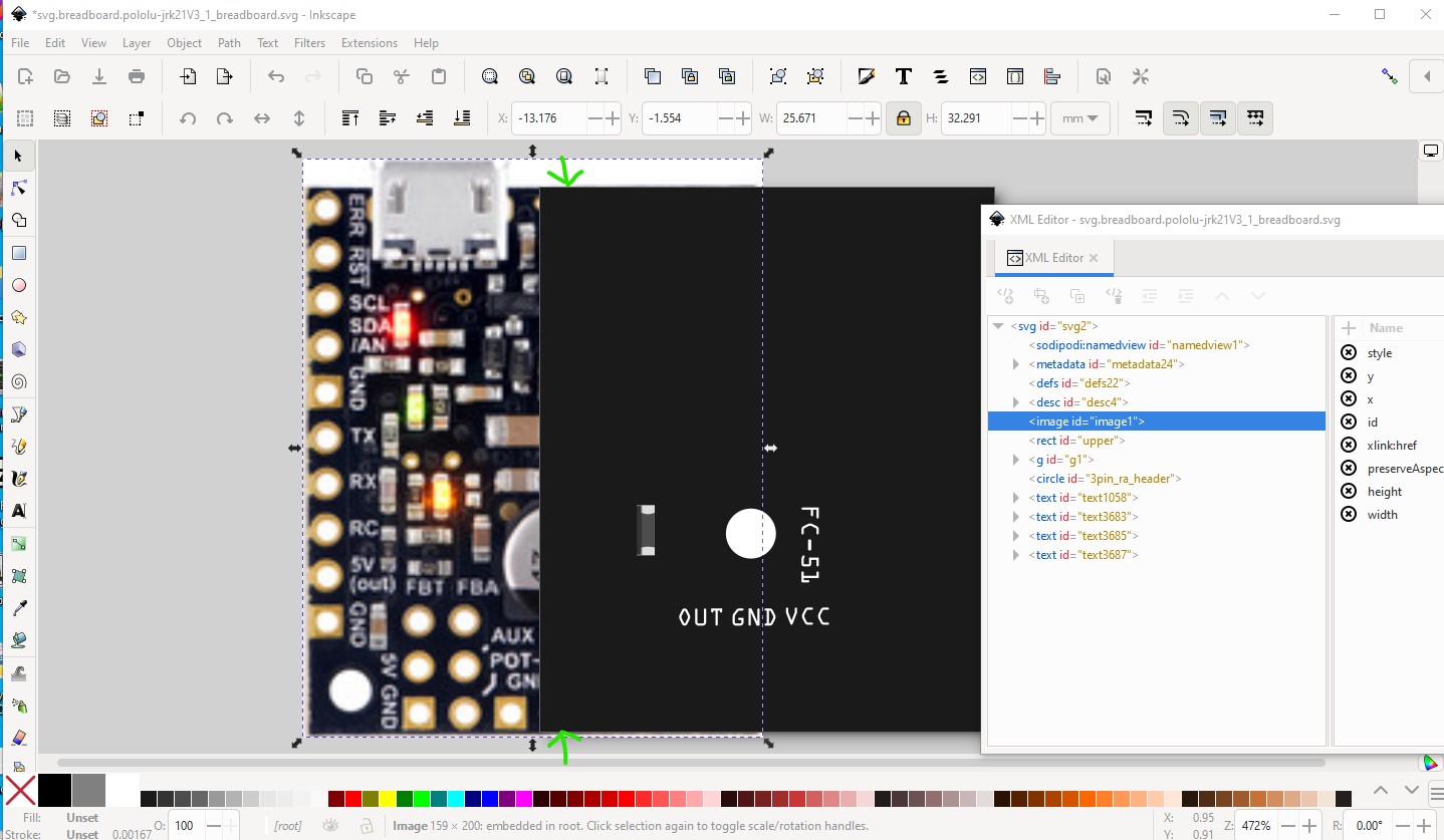
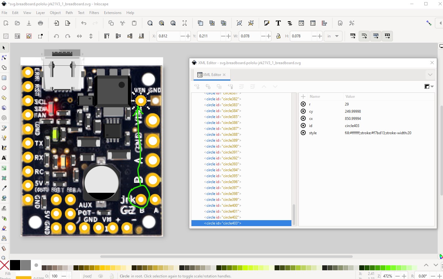
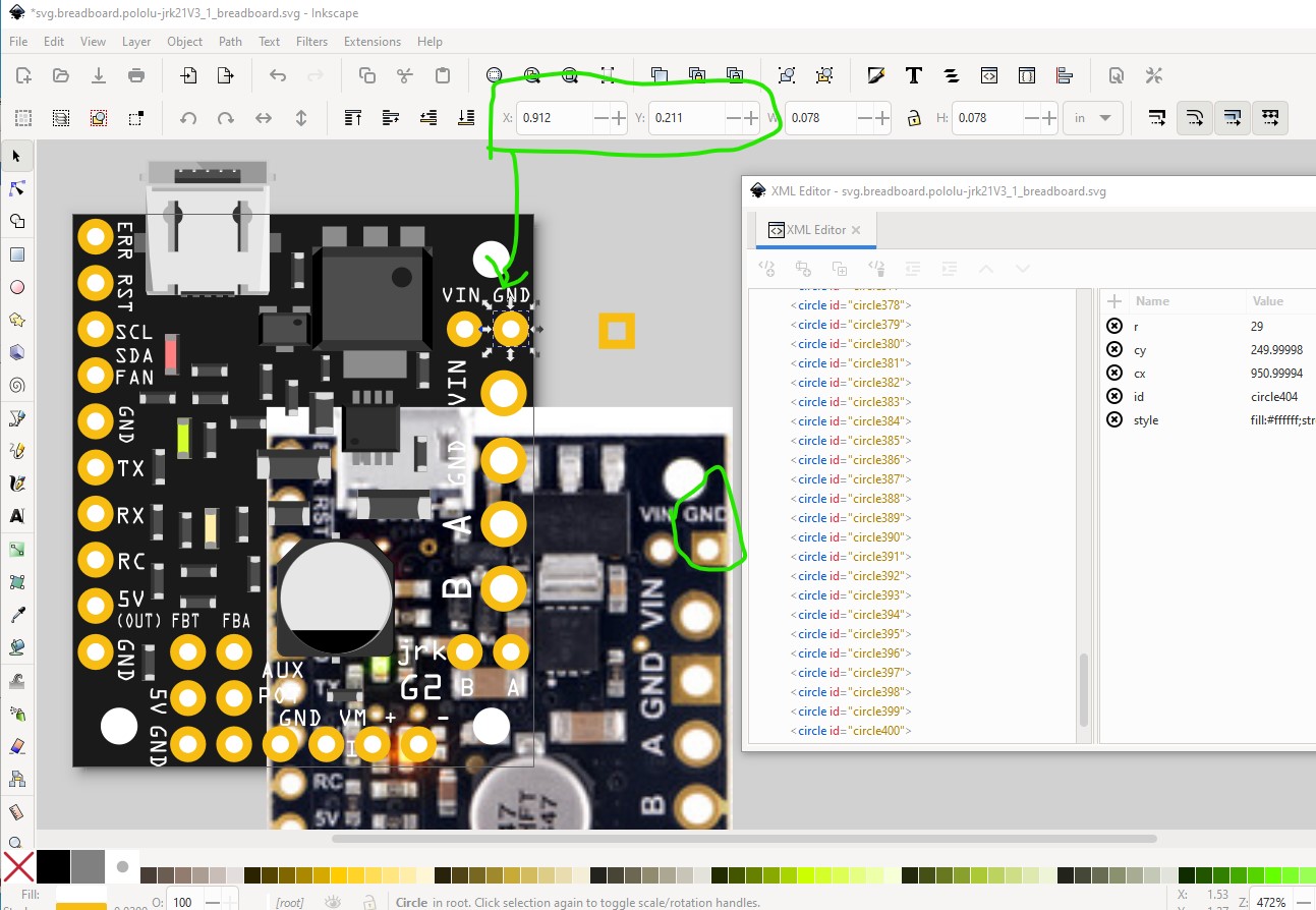
now create the squares for the pads that need them (should have done this first, but you need the pads to place them anyway.) Move the jpeg out a bit to identify which pads need squares.
set the square to the same height and width as the associated pad then move the square to the same coords as the associated pad.
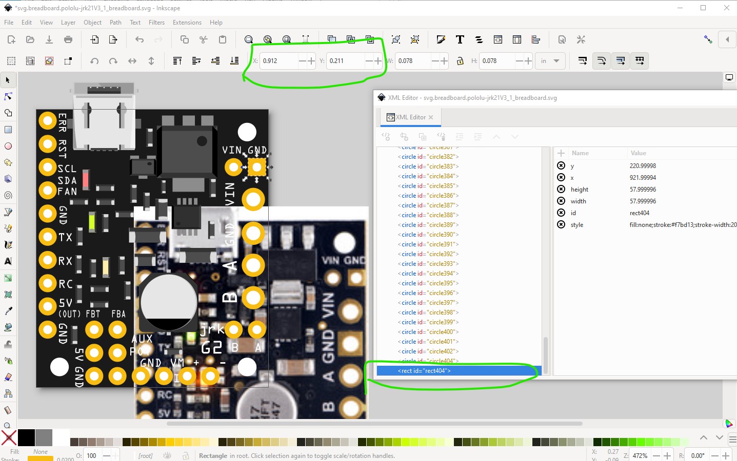
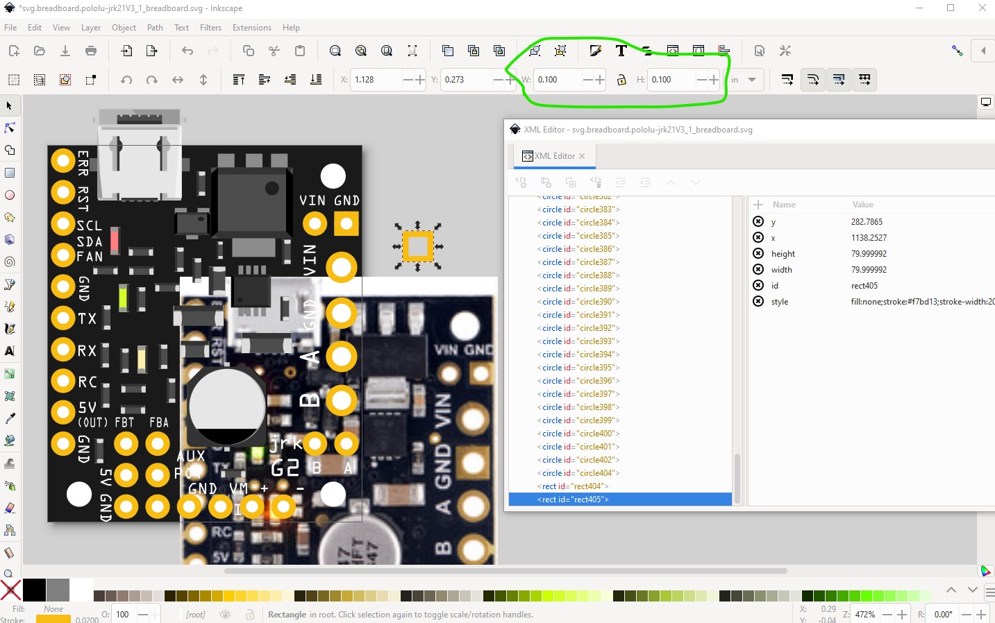
do the same for the larger pads
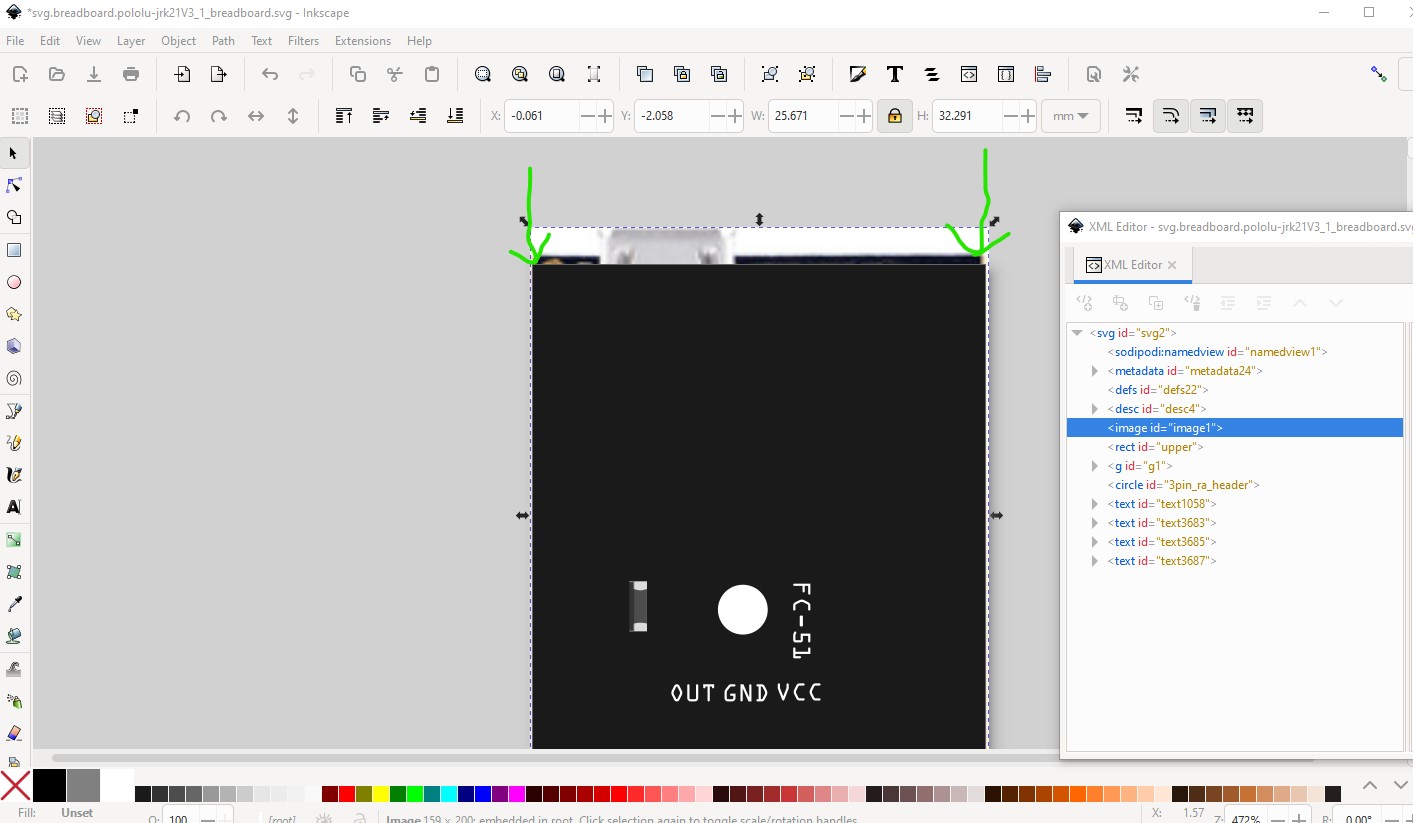
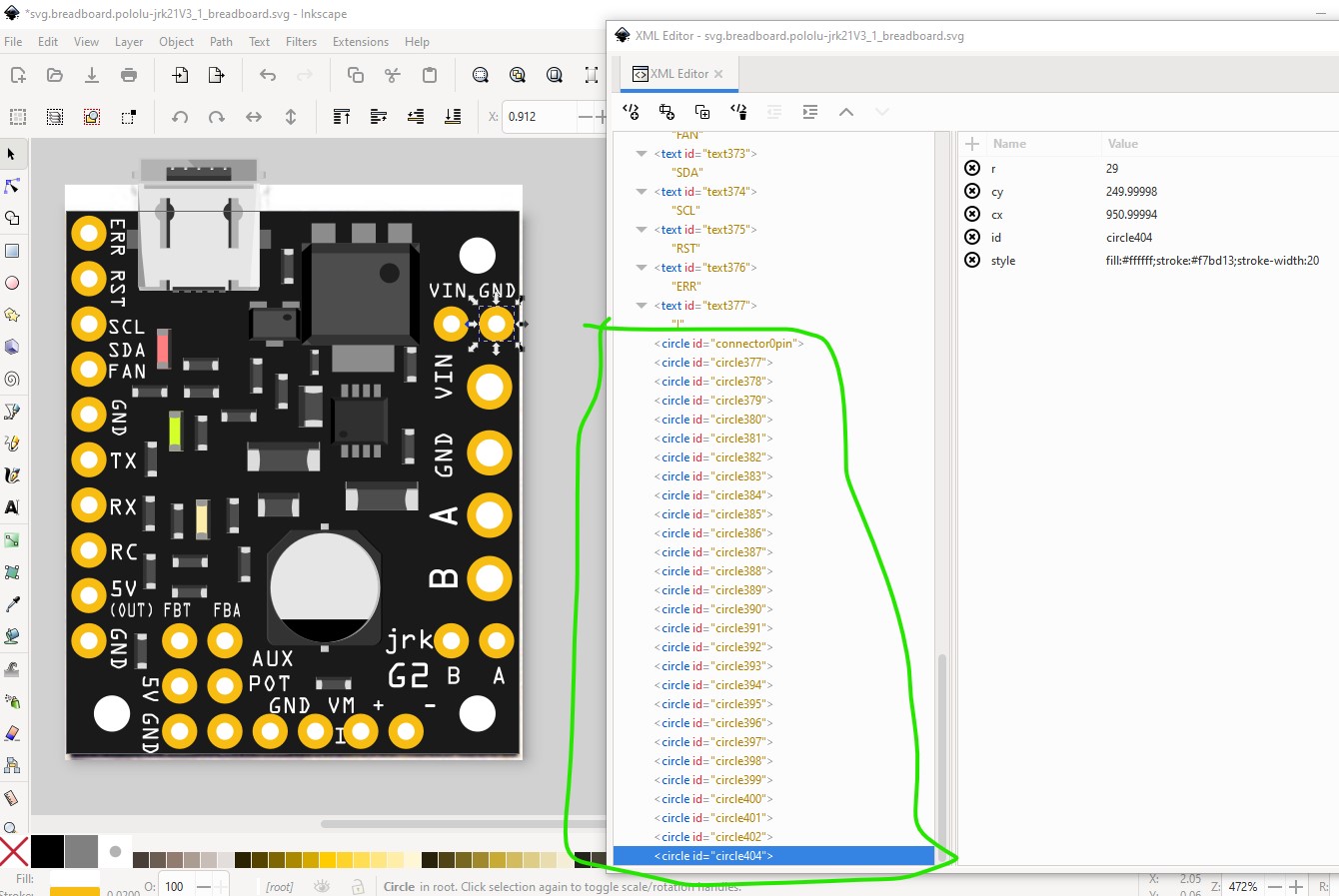
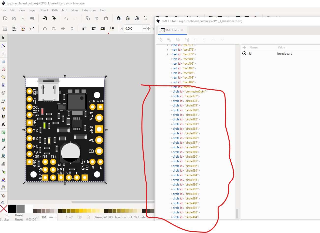
when finished move the square up so the connectors are the last thing in the svg.
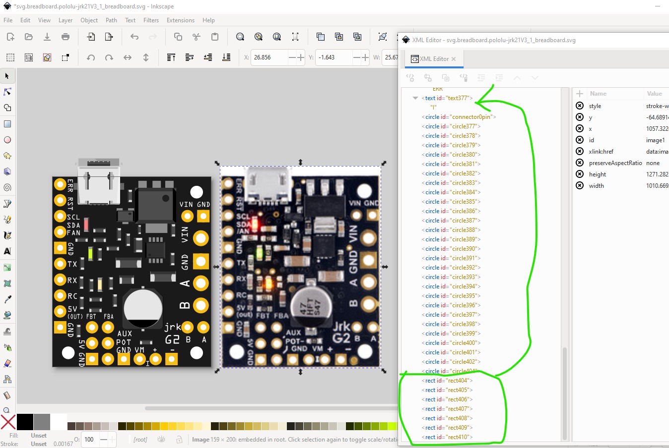
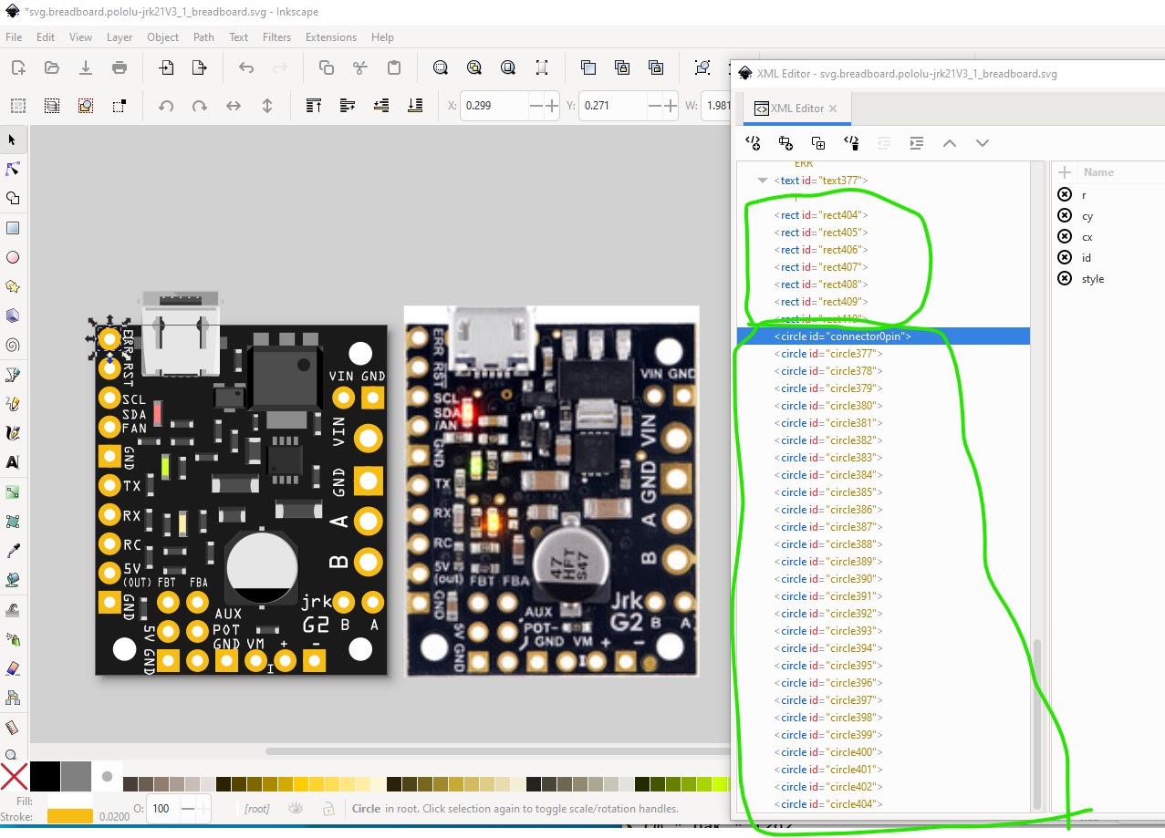
leaving only the circles for the connectors at the bottom of the svg.
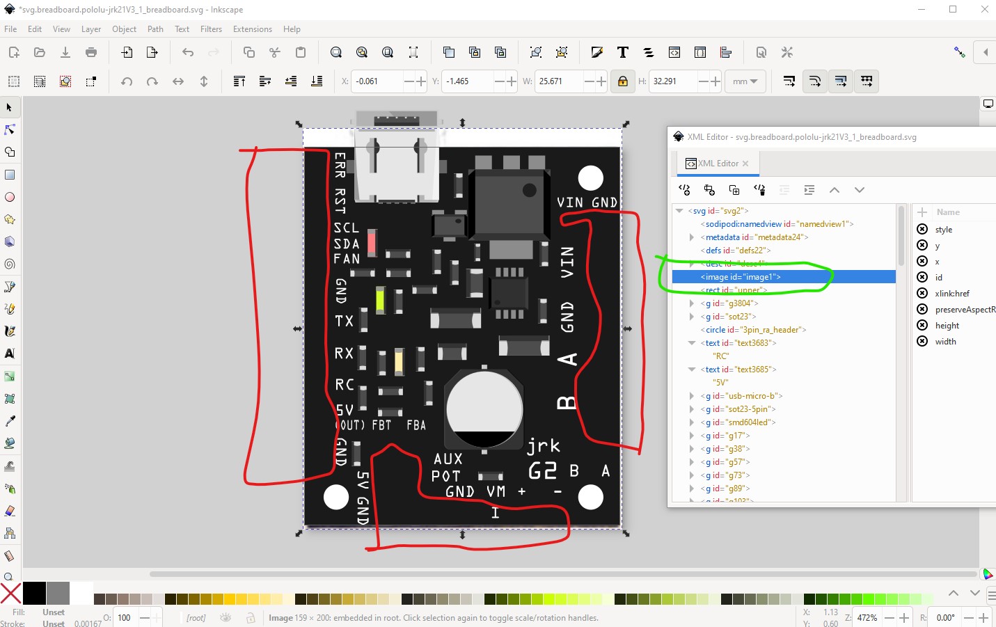
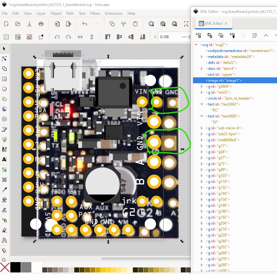
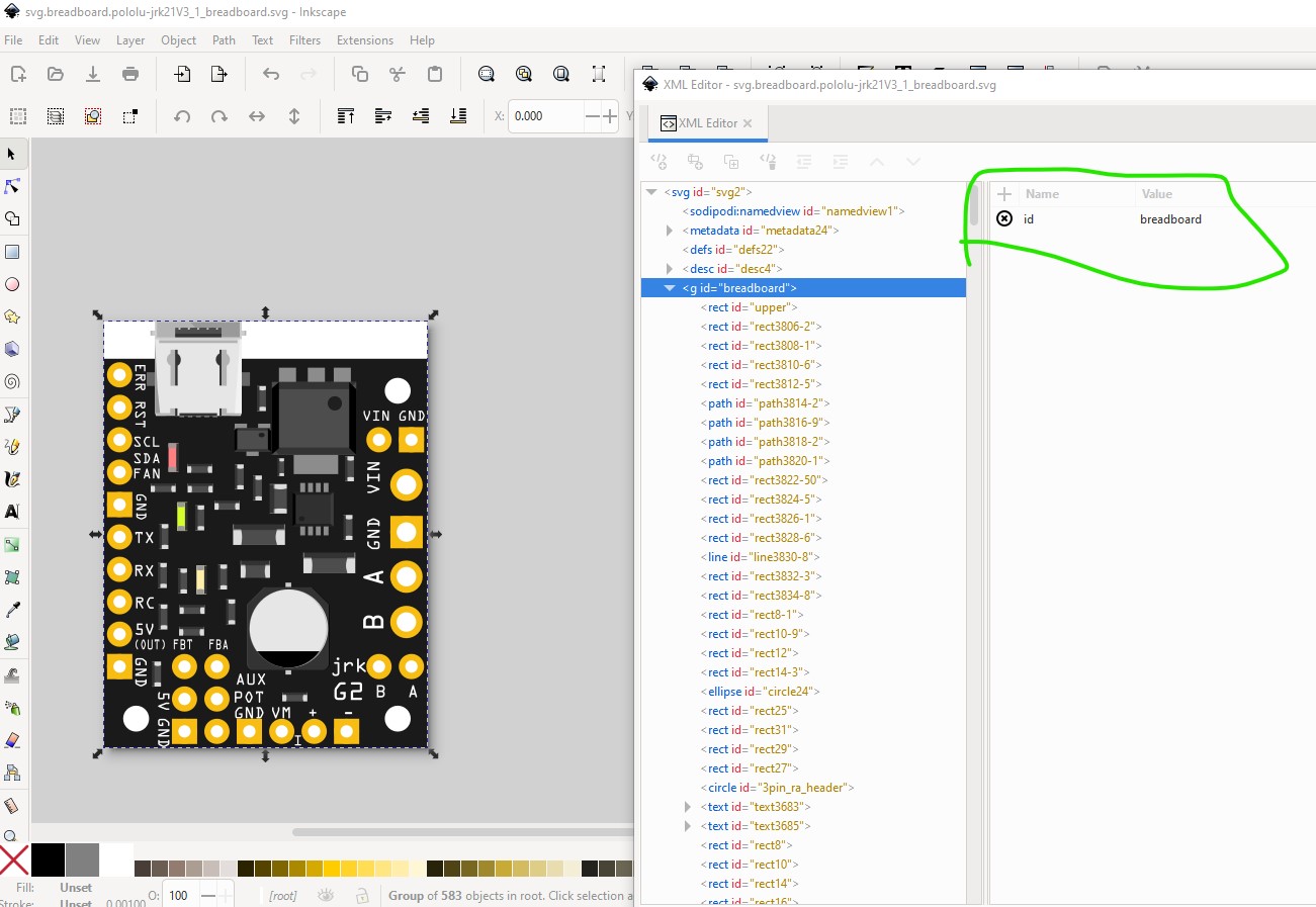
delete the jpg image, then do edit select all and group to group the entire svg
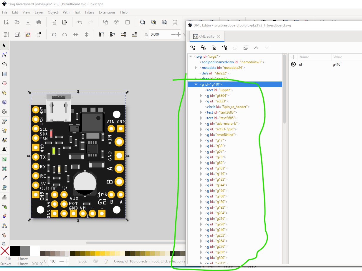
select the resulting group and hit alt-cntrl-g to ungroup multiple times to ungroup everything in the svg. Then do edit->select all and edit->resize image to selection to resize the viewbox,
then group the entire svg to create the breadboard layerid. and set its id to “breadboard”
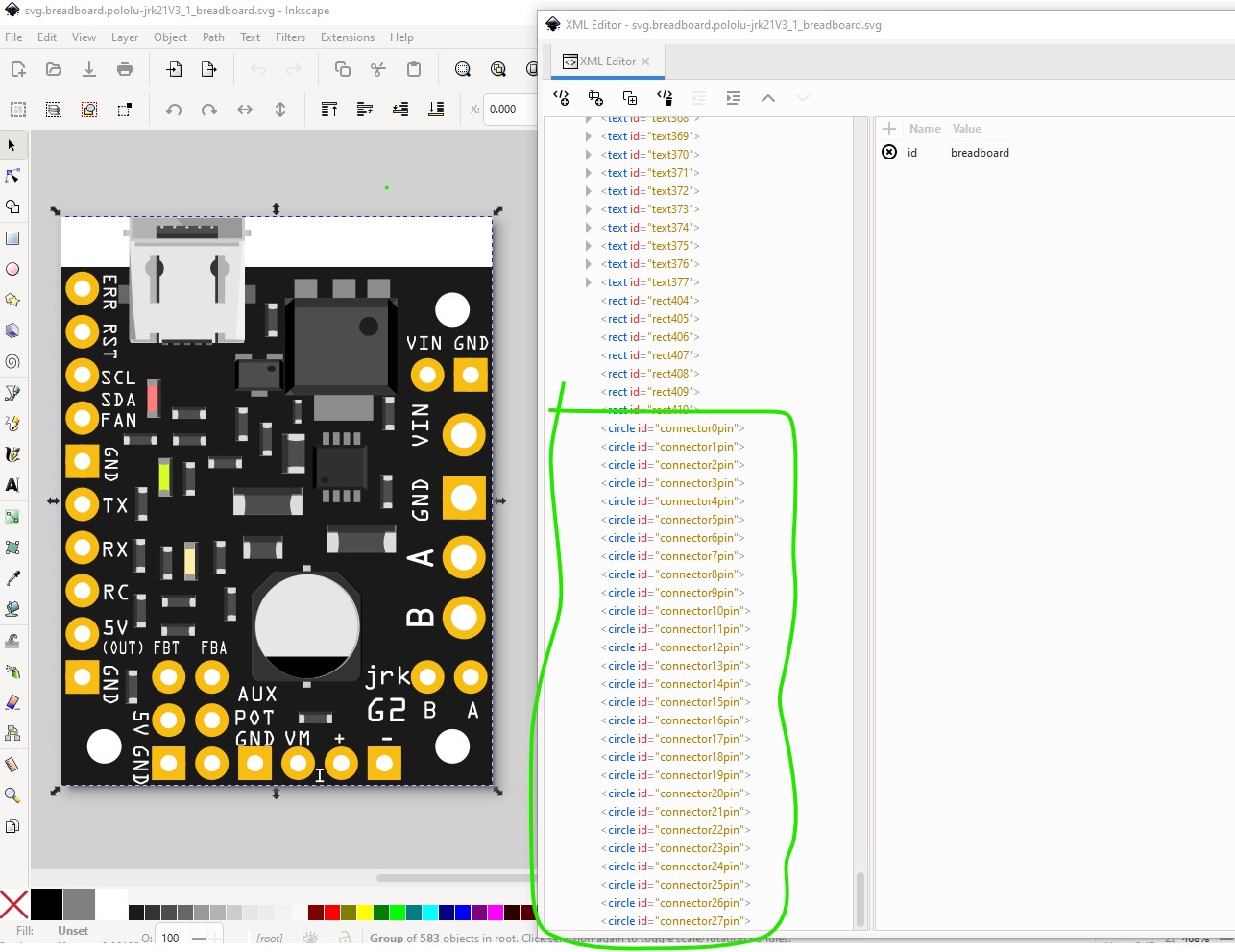
that leaves the connections at the bottom of the svg ready to be renumbered. Run a python script to renumber to connectors.
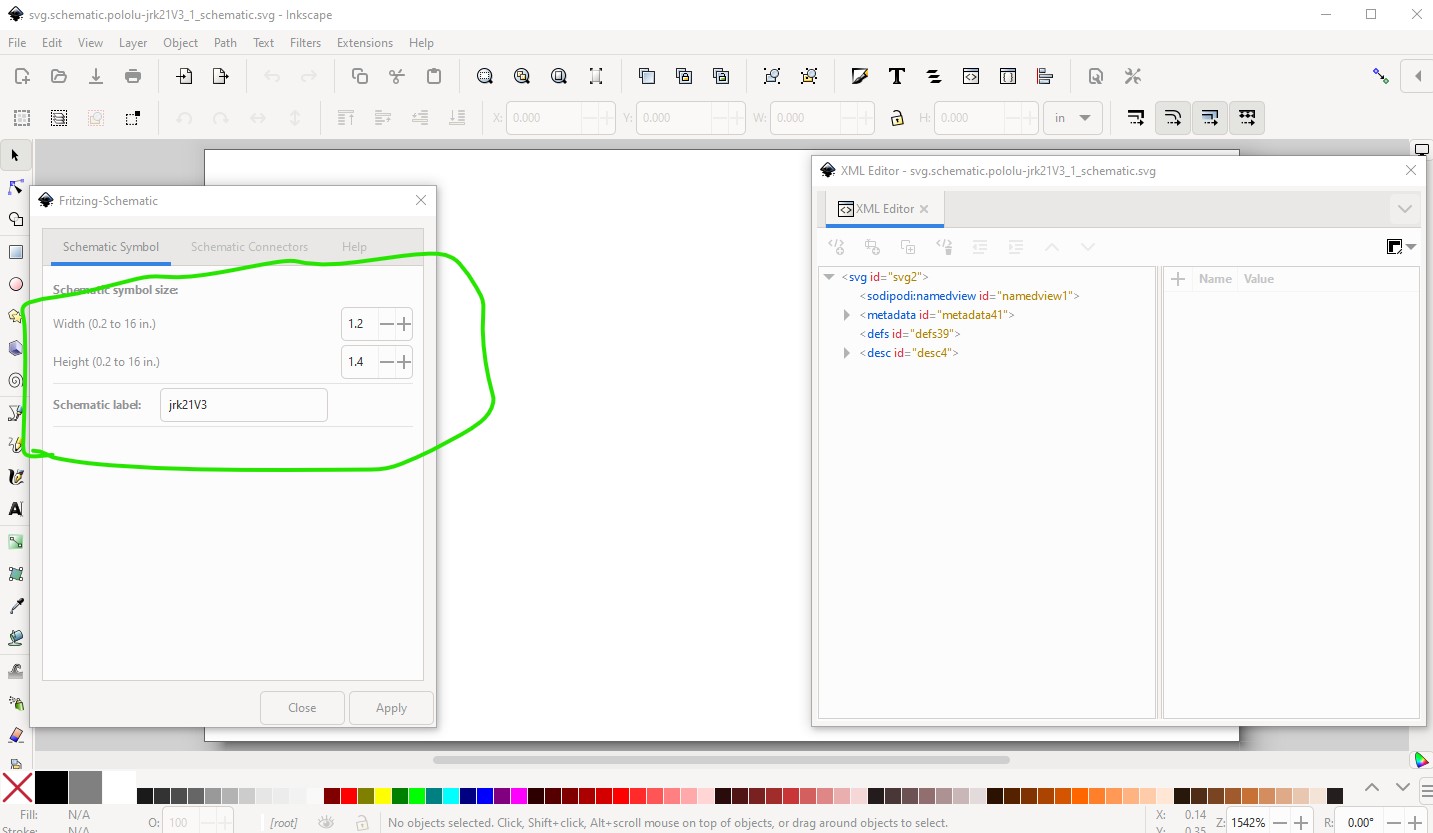
then save the breadboard svg because it is complete. Now move on to creating schematic. Use Randy’s schematic extension for Inkscape to do so. First set the required parameters
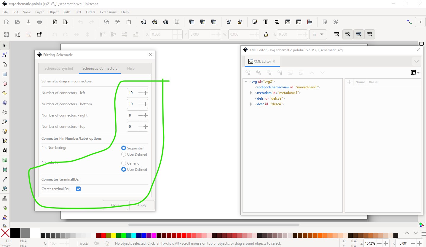
then click apply which brings up the left side pin labels. Set the labels to the appropriator values then click finished.
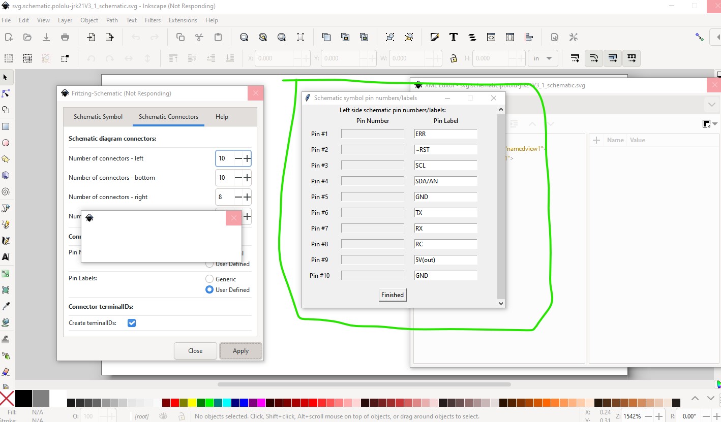
repeat for the bottom pins
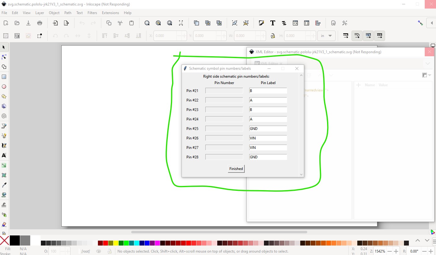
and then the right pins
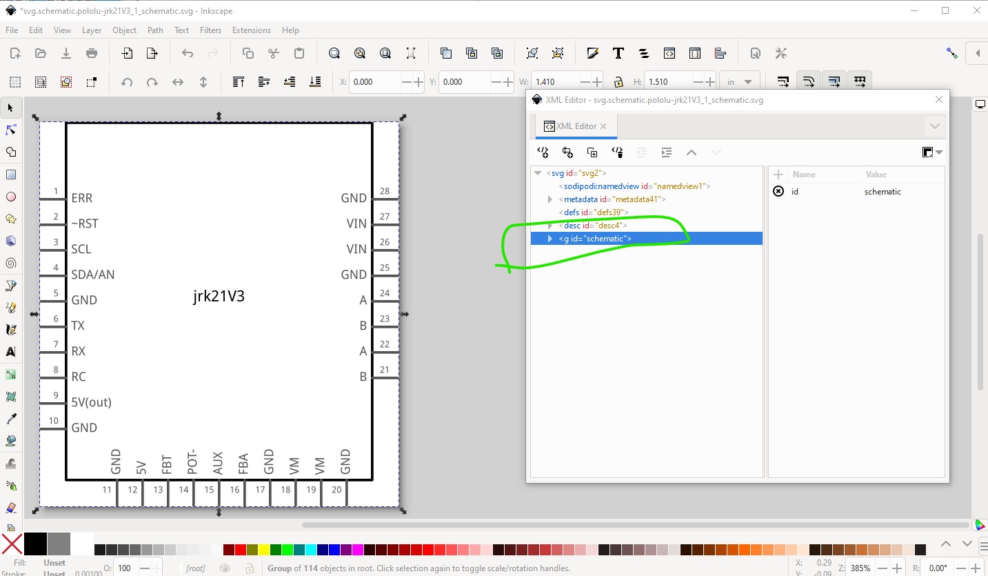
now ungroup the schematic because we need to move pins around.
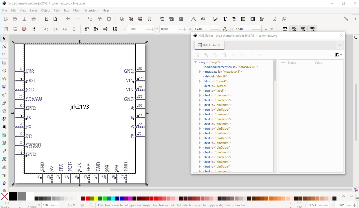
separate the various pin groupings (as usual I had to increase the size of the rectangle to do this!)
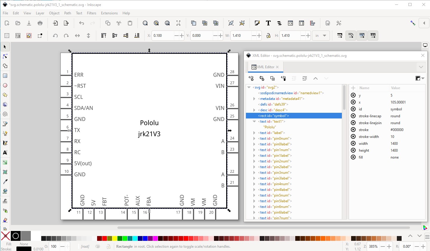
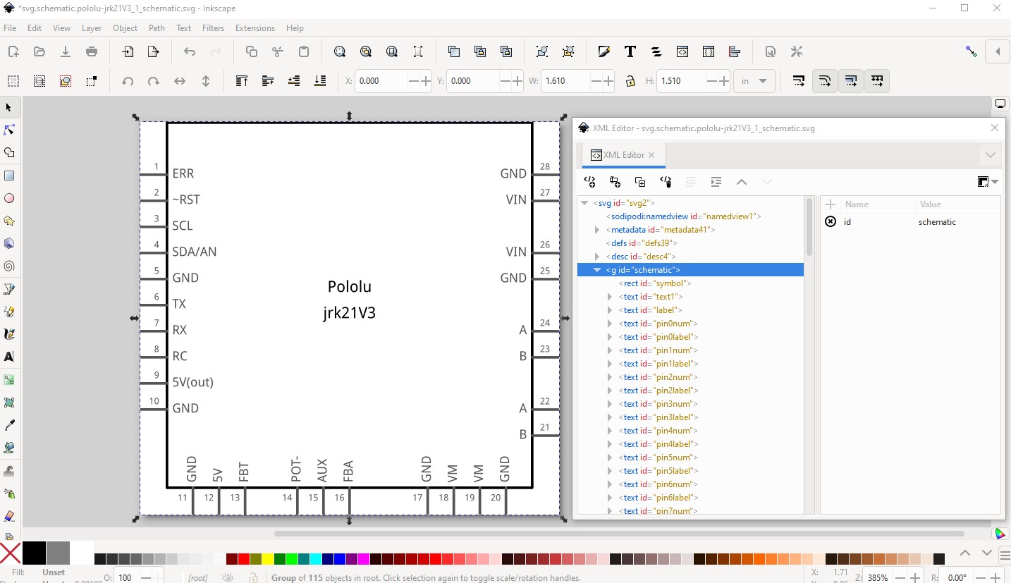
the editi->select all and group and reset the schematic layerid and save the svg. Now on to pcb. Copy the breadboard svg to the pcb svg like this
ungroup it and delete all the components
then convert the rectanlge to an outline and change the mounting holes from white to black.
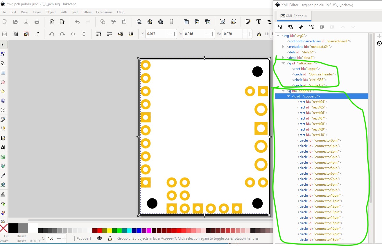
edit-select all then edit-> resize page to selection to reset the view box then group the elements in silkscreen
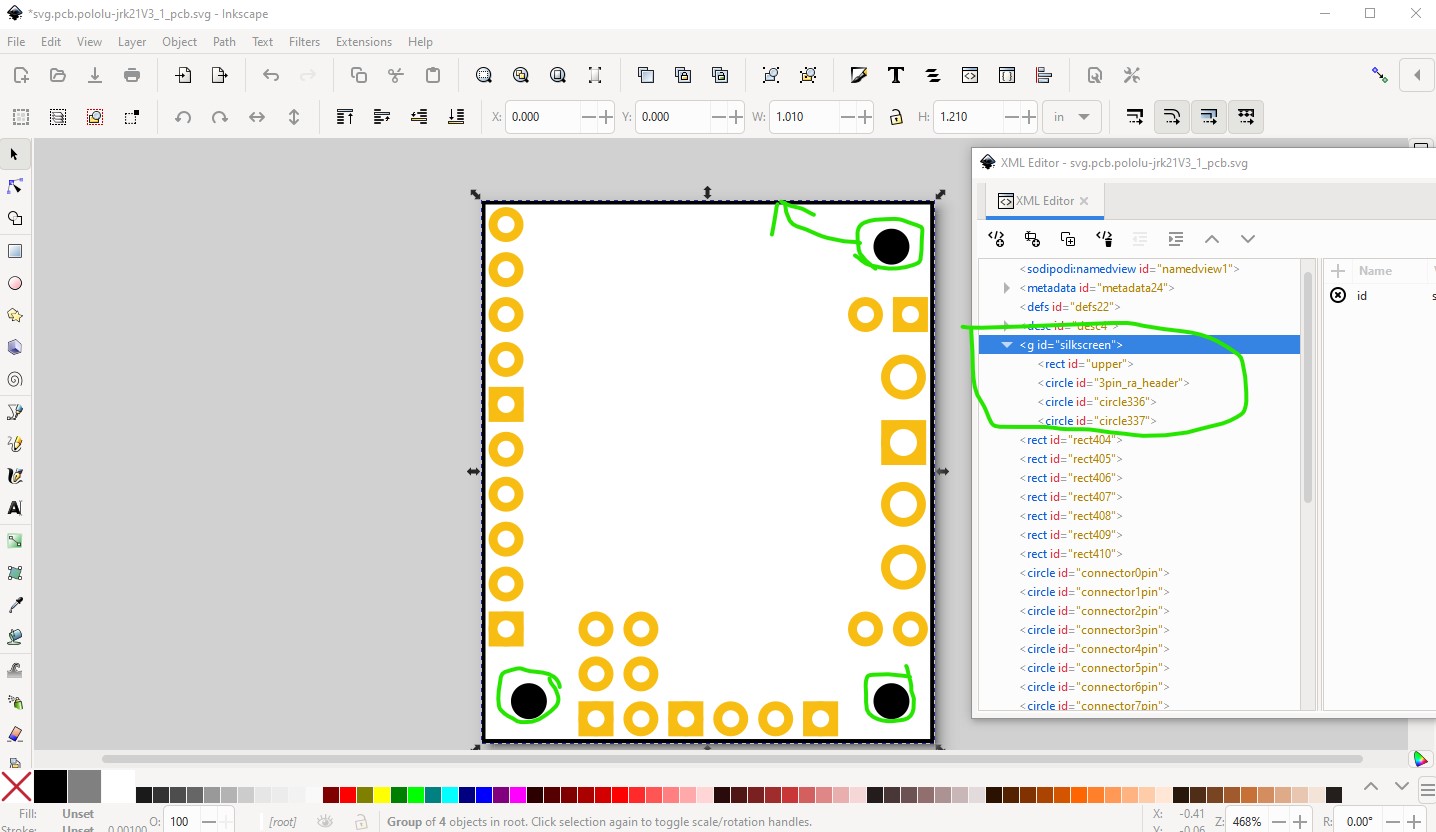
do the same to the connectors and set the groups to copper1 and copper0 like this
and save the pcb svg. The svgs being finished, now create the .fzp file and set it appropriately and the part is complete. Run it through FritzingCheckPart.py to verify all is well, then test it tom make sure all works correctly resulting in the part at the start of this post.
Peter
Thanks Peter ![]()
![]() for your work and explanation!
for your work and explanation!
What would the forum be without your help?