Does anyone have or willing to create a relay, part number HK19F?
The spacing is .1in so perfect for breadboard projects.
Does anyone have or willing to create a relay, part number HK19F?
The spacing is .1in so perfect for breadboard projects.
I found the following which is the same layout but with different pin spacing.
It looks like @steelgoose was kind enough to assist correcting an error with that part.
I thought I could copy that part and correct the pin spacing. It looks like the part would need to be edited in an SVG editor as the changes cannot be made from within the parts editor of fritzing. Am I missing something?
Sorry if this is a dumb question, but I was trying to avoid having to learn two new apps at the same time.
Yeah. You have to unzip it and mod the svgs.
I guess what you are trying to say… you want me to make the part for you.
All three .svg’s need to be redrawn in a graphics editor, it would be very difficult to fix it in a XML editor.
[quote=“steelgoose, post:4, topic:2003, full:true”]
I guess what you are trying to say… you want me to make the part for you.[/quote]
It would be great if you could, but also understand if you don’t have the time.
If you were to do it, what would be your approach? Are you saying it would be easier to effectively start from scratch? Or a combination of editing the 3 svg files and then editing the XML file? If the second approach would the XML file be edited within the editor program or are you talking about editing the file in a text editor.
Do you have svg drawing experience, as it actually takes longer to explain it than to do it.
Only some things you can do in the xml editor… moving thing and sizing is not one of them. You can change name, numbers, some times the size, etc. Sometimes the format of the .svg, you don’t even know what it is. Trying to build a part from nearly scratch would take a lot of calculations. Much easier to fix it in a graphics editor.
I will work on it tonight, it is no big deal. I guess you are going to solder it through hole. I see that it has 1mm diameter pins.
[quote=“steelgoose, post:7, topic:2003, full:true”]
Only some things you can do in the xml editor… moving thing and sizing is not one of them. You can change name, numbers, some times the size, etc. Sometimes the format of the .svg, you don’t even know what it is. Trying to build a part from nearly scratch would take a lot of calculations. Much easier to fix it in a graphics editor. [/quote]
Thanks, I appreciate the help and education. I hope once I get up to speed I can pay it forward.
[quote=“steelgoose, post:7, topic:2003, full:true”]
I will work on it tonight, it is no big deal. I guess you are going to solder it through hole. I see that it has 1mm diameter pins.[/quote]
Thanks, I really appreciate it. Yes, going to solder through hole on stripboard for prototype (a little tight but they do fit) and then PCB for final product.
Got it, maybe I will earn another brownie button… I would rather do this than to watch presidential politics on TV…
What are you making?
I’m with you on presidential politics.
It’s combing a couple of circuits for a car project, a dc-dc circuit, a couple of relays, an arduino nano and a few switch inputs.
Here is your part, check it over, I think I have everything right.
Relay-HK19F.fzpz (11.9 KB)
Good luck with your project…
Thank you so much, it looks perfect. Actually you also saved me from another mistake, on my hand drawn diagrams (well powerpoint) I had the center pins as the commons and not the pins closest to the coil as you correctly identified.
Thanks for the brownie buttons… maybe one of these days I will make Eagle Scout… 
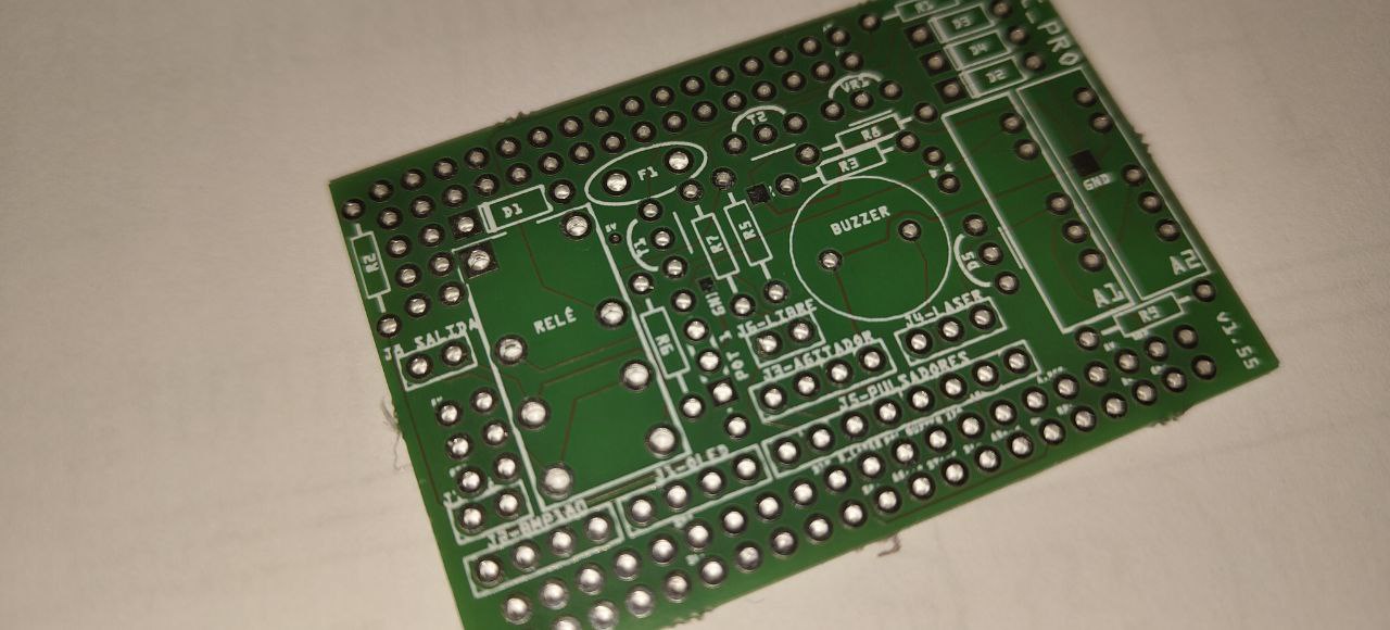
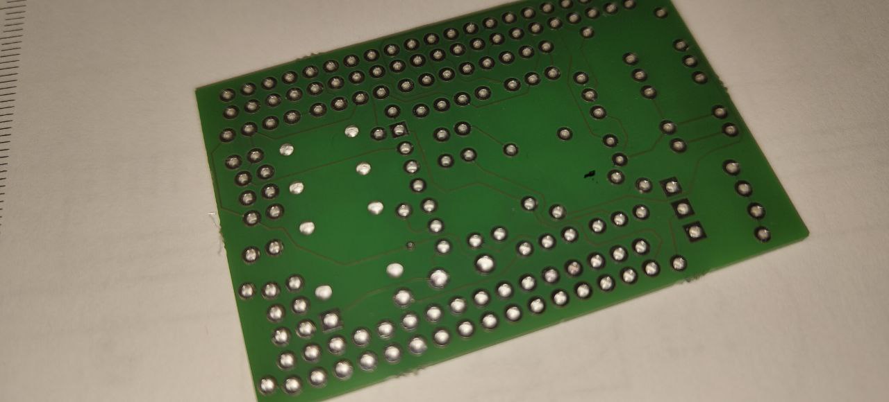
I have a problem with this component. it only shows up correctly on one side of the pcb and it is not easy to solder it in.
Can someone help me?
On this side of the PCB it is correct…
Notice how the relay holes do not have enough coverage to be able to solder.
I add photos of the problem…
The part is incorrect.
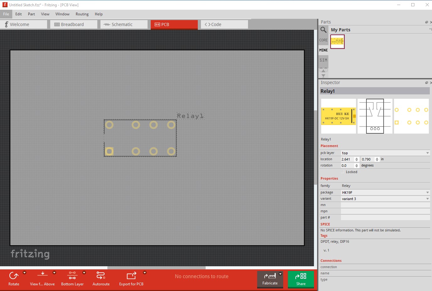
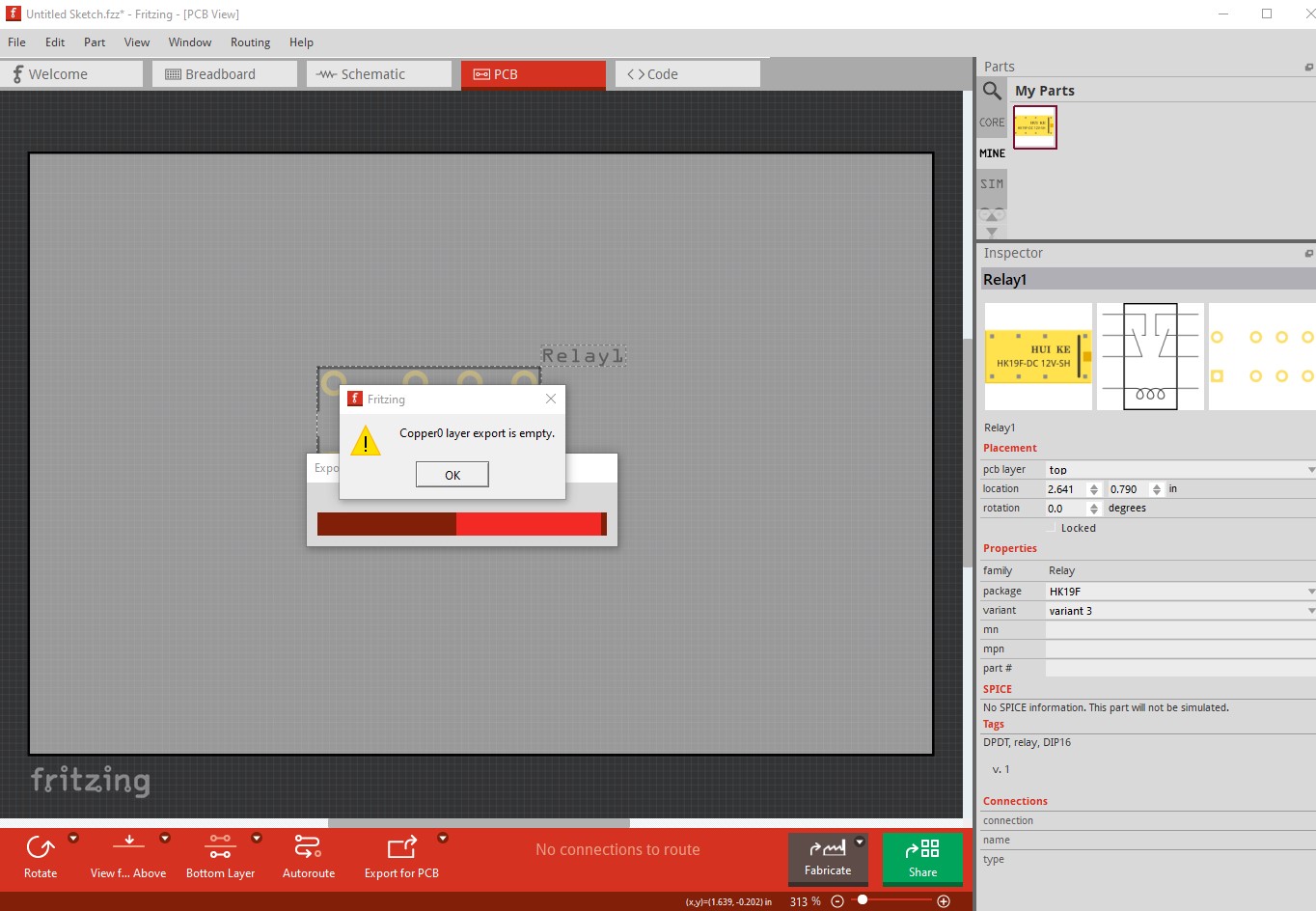
Here in Fritzng we pcb view we see there is no bottom layer pads.
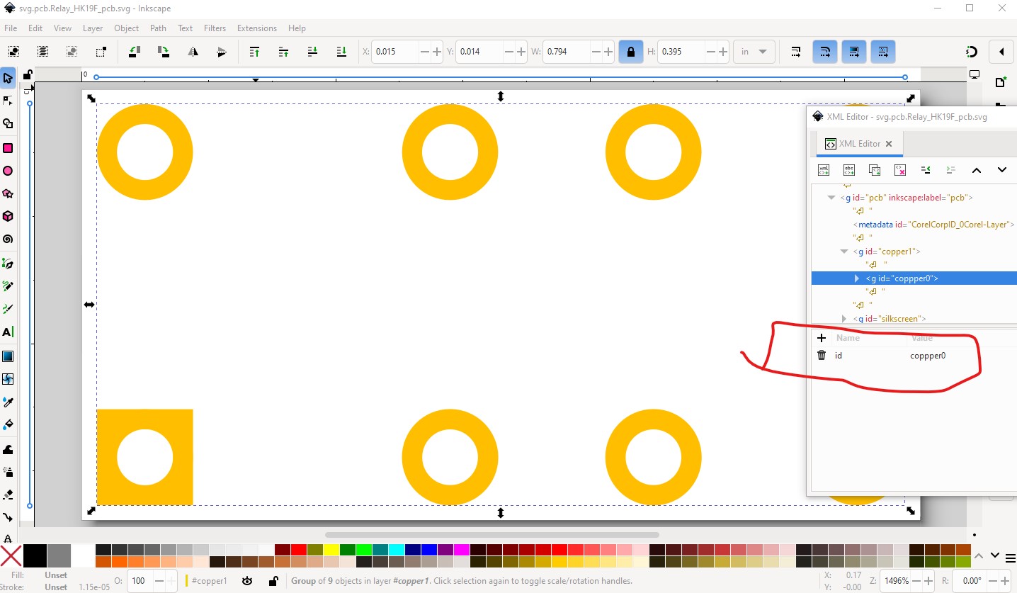
when I export only the part as gerbers Fritzing complains about no copper0 layer
editing the pcb svg in Inkscape indicates the problem is a typo in the copper0 layerId.
The pcb copper0 layer was named coppper0 and thus won’t appear on the bottom layer. As well the holes are too large. Here is a part with those two errors corrected. I didn’t change the moduleId so you will need to delete the current part from your mine parts bin by selecting it, right clicking and click remove part. You then need to shut down Fritzing and answer yes to save parts and save parts bin to really delete the part before you will be able to load this part in to Fritzing. The new holes are the recommended 1mm from the data sheet here:
Relay-HK19F-fixed.fzpz (12.2 KB)
Peter
Thanks very much!!
I knew something was up. ![]()