I went lazy for the schematic and pcb view for now but atleast I finished (I think) the breadboard view. I know it hasn’t been rescaled but I just want to read your opinions.
Looks fabulous! You are much better at the graphic art side of this than I am, hopefully we can convince you to keep making parts . I only see two issues at a quick look both connector related: it is desirable (but not the case in many parts) that connectors start at 0 and go up in sequence to the number of pins-1 which isn’t so far the case here. The reason is that Fritzing is expecting (and assumes) the next pin will be sequential when it creates the labels from the fzp file. If you have connector6 (pin 7) label x, no connector 7 and connector 9 (pin 10) label y if you hover on the pin in breadboard pin 7 will show label x, pin 10 show pin8 (which doesn’t exist) and I think a random label (it may be pin 11 which will show the random label) and then it will recover and label the pins properly. A minor issue but annoying and not correct. The other issue is that at least connector16 and 17 on the battery plug aren’t on the .1 grid, but over all a beautiful job.
Any zip program should open 7zip files perhaps unless he used the .7z format. By default in my case 7zip uses .zip format but I have seen .7z files which 7zip happily reads but other packages may not.
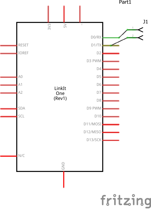
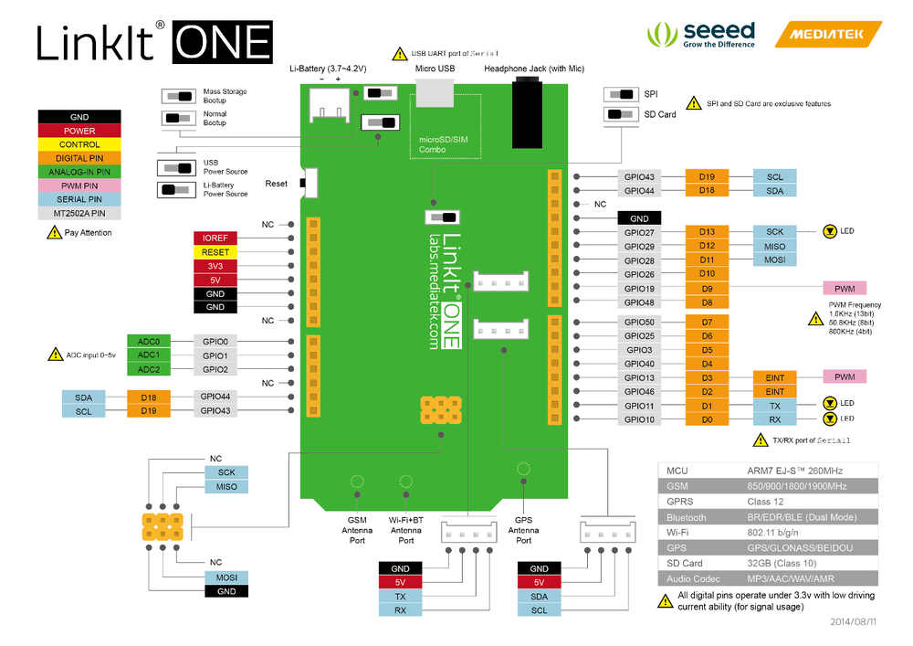
I’m not sure that is correct. This board is a CPU and has its own pin names that may or may not match the UNO. I’d be inclined to use the labels on the LinkIt pinout page (which of the several for each pin is an issue though ) so it matches the documentation for the board because that is likely what the user will refer to.
Sorry, what I meant was that if you add a the std UNO BB svg into a new part with Part Editor and it AUTO assigns then that part should auto assign because it is an extended UNO. All you just have to relabel the names in Connector. If it doesn’t auto assign then then it doesn’t matter.
Basically I was thinking if UNO svgs auto assigns and you modify the 3 UNO svg and it would already be assigned when added to a new part. But if that’s not the case it’s not many pins to assign.
Damn I don’t have 7zip and it won’t unpack. Should have Send to Compressed folder in Win.
Thanks! Well based on Old_Grey original .svg file, I let the same pin names because that is the last thing to do after finishing a piece. Now I will take a look at the pinout diagram and assign the correct label / terminal id using xml.
I always struggle using the correct grid on Inkscape. I will post my program settings (Inkscape):
For this one I use
x, y spacing: (.01,.01)
Primary line each: 10
which when zoomed way in gives a 10 thou grid and when zoomed out to normal size creates a .1 in grid. You can then move the x/y start positions so the grid matches one of the connectors and the rest of the connectors should then align on the grid if they are correct. In practice though to check pin alignment I usually set the tool bar to in and read the x/y starting position of one pin then make sure all the rest are an exact .1 multiple from those x/y coords (changing the x/y in the tool bar if they aren’t). I often find snap to grid more annoyance than help and tend to disable it sometimes. As I’ve noted I’m not very good at svg editing (I learned it along with parts making) so there is almost certainly a better way to do this than how I do it.
But I really can’t get it to fit perfectly the .1 grid thing, not sure why, I always check it on Inkscape but on Fritzing, it has a little offset thing when importing it.
MAKE SURE YOU CHECK THE PCB FOOTPRINT BEFORE GETTING PCBs MADE BECAUSE IT WAS MADE WITHOUT A DATASHEET AND GUESSED THAT IT IS AN EXTENDED UNO FOOTPRINT.
I think the grid starts at the edge of the page size so you make it a touch bigger until it lines up.
You usually ‘select all’ and ‘resize page to selection’, but in doc properties you can adjust the margins of the page size.
I think fzbz is the whole bin, but you can right-click on a part and individually export it and it becaomes fzpz
Yah, that was my reaction too . Now on to the faults. Breadboard alignment is fairly easy. The connectors are different sizes connector0pin is w 0.056 h 0.056 connector46 and 47 (and the grove connectors) are w 0.020 h 0.019. This matters to alignment because grid alignment is to the center of the pin, however drawing alignment is to the bottom left corner. I just discovered that in Inkscape if I select the xml editor window and type connector0 it will find and highlight connector0 in the xml editor! In any case back to alignment problems. Connector0pin is
x 2.495 y 1.972 w 0.056 h 0.056 so pin center is x 2.518 (x 2.495 + (w 0.056 / 2) and y center is 1.995 (y 1.972 + (h 0.056 / 2). So far so good, all the rest of the connectors in that row are .1 apart and all is well. Now we hit connector46 and do the same calculation: x 0.200 y 0.290 w .020 h .020 (round up from the real .019 for ease of math) which gives a center position of x 0.210 (same calculation as for pin 0 but different width) and y 0.30. As we see the center of pin 46 is not on a .1 grid compared to pin 0, and thus we have the misalignment in breadboard. My preferred fix is to change all the pin height/widths to the same value but doing so will change there x/y position (as the calculation still starts from the x/y values but the width and height are smaller meaning we need to add some (which can be calculated) value to the x/y coords to keep the pin in the correct place. The correct way to automate this would be to use a python script to do it (unless someone knows an Inkscape way of doing it which i would love to hear!) or in the short term do it manually which is a fair bit of work. If you do it manually do the 2 grove connectors and the power connector as there are less of them than the headers. Next issue is the schematic svg. As a personal preference I like to have schematic (as much as possible) mimic the breadboard view, so I would structure schematic like this:
bat con+ |-------------------| first grove pin 4
bat con- |-------------------| …
_________|-------------------| first grove pin 1
header8pin|----------------| second grove pin 4
… |___________| …
header1pin|| second grove pin 1
(if this isn’t clear I can create a proper svg the forum is formating this oddly). The other issue is your schematic terminalIds are missing in the fzp file for some of the pins. Connector0 is good:
p terminalId=“connector0terminal” layer=“schematic” svgId=“connector0pin”
connector1 is wrong (no terminal id which makes the line connect to the center of the pin rather than the end in schematic):
p layer=“schematic” svgId=“connector1pin”
and last, it is preferable to export the part as an fzpz file rather than an fzbz file. Here is a png of connector0 (works) and connector1 (no terminalId) to show the issue and how to test for it in a sketch which testing your part:
If you connect the header straight in to the pin on the board it will appear to work even though it is wrong due to the lack of a terminalId.
Edit: Just remembered one more issue: The VCC and GND (and perhaps other) pins need to be bused either via editing the fzp file or setting internal connections in parts editor.
Pin connectors are straight off the UNO, and we know most parts aren’t prefect, but then again it’s not supposed to fit on a 0.100" breadboard, like an UNO, so maybe it will do as is.
I had to google "grove connector in order to understand what part you were referring to. Connector46/47 were based on grove connector provided by Old_Grey
Basically Fritzing doesn’t place the drawning wires at the connector middle point (x,y) but instead to one of the corner (Bottom left). I had no idea about it
What? I was looking for such feature as search bar but never found it.
New tip of the day
You mean connect them together using internal connection, so they get highlighted if something is connected like “GND pin 1” and “GND pin 2” as example?.
What I should do? Move the yellow header to fit 0.1" grid or let it be?
But if I fix the breadboard alignment, I should fix the pin alignment too
If you node select - under arrow select - in INK and click on an object in the drawing it will highlight in the XML dialogue.
This part can’t connect to a breadboard in real life so it doesn’t have to align with a BB. You should use it like an UNO and use wires to connect to it.
This is going to be a very low demand part - it’s expensive, so maybe less than 20 -, so if it works leave it as is.
We should do a new topic about standard measures when making a part in fritzing
This topic should include all information regarding how to setup grid, units and so on inside Inkscape (or illustrator). Of course some exception like these board when using on fritzing enviroment.
Not quite. It is a difference in opinion between Inkscape and Fritzing. Inkscape starts an item at the bottom left corner (that is 0 0 in Inkscape coord space. Frizting connects to the center of the item in terms of the grid (it may use Inkscapes values for the coords of the item). That means that Fritzing calculates the grid based on the middle of the item but Inkscape adjusts the item based on the bottom left corner causing the offset you are seeing. If all the terminals are the same width and height both sides are happy, as long as the start x/y coords of a terminal of identical size are on .1 boundaries the alignment will be correct. The problem you are seeing is because the header connectors are 0.056 wide and high and the grove connector ones are 0.020 wide and high (or almost). That means if connector47 starts at the .1 in grid boundary as connector0 on the header, the center of connector47 will be offset .036in in x and y from the center of connector0 causing the misalignment you are seeing.
I’ve been fighting with Inkscape for close to 2 years now and just found it . I have stumbled across it before a couple of times but never figured out before now how to trigger it intentionally.
Yep, that’s it. You want all the pins that connect together internally to be bused so the Fritzing part acts like the real part.
Since you are putting the effort in to making the part, the choice is yours. It will work as is, and that is the easiest solution. I’d prefer to fix up the connectors to all be on the .1 grid so the part looks its best, but that will be a bit of work (easiest is to either change the size of the terminals in the grove connectors as there are less of them or do the calculations to move the center of the existing pins on to the .1 grid like the rest of them).
That is probably a good idea, because if we can get agreement on guidelines that would help with part consistancy. That said there aren’t at the moment that many of us even making parts.
We actually had this conversation before. Some people wanted to make everything BB connectable, but I had the impression that FZ creators wanted BB view to be real world so very young children can get into electronics easily because they copy what they see. If real world wasn’t the intention what’s the purpose of the BB view, because you already have a non real world representation in the SCH view.

 . I only see two issues at a quick look both connector related: it is desirable (but not the case in many parts) that connectors start at 0 and go up in sequence to the number of pins-1 which isn’t so far the case here. The reason is that Fritzing is expecting (and assumes) the next pin will be sequential when it creates the labels from the fzp file. If you have connector6 (pin 7) label x, no connector 7 and connector 9 (pin 10) label y if you hover on the pin in breadboard pin 7 will show label x, pin 10 show pin8 (which doesn’t exist) and I think a random label (it may be pin 11 which will show the random label) and then it will recover and label the pins properly. A minor issue but annoying and not correct. The other issue is that at least connector16 and 17 on the battery plug aren’t on the .1 grid, but over all a beautiful job.
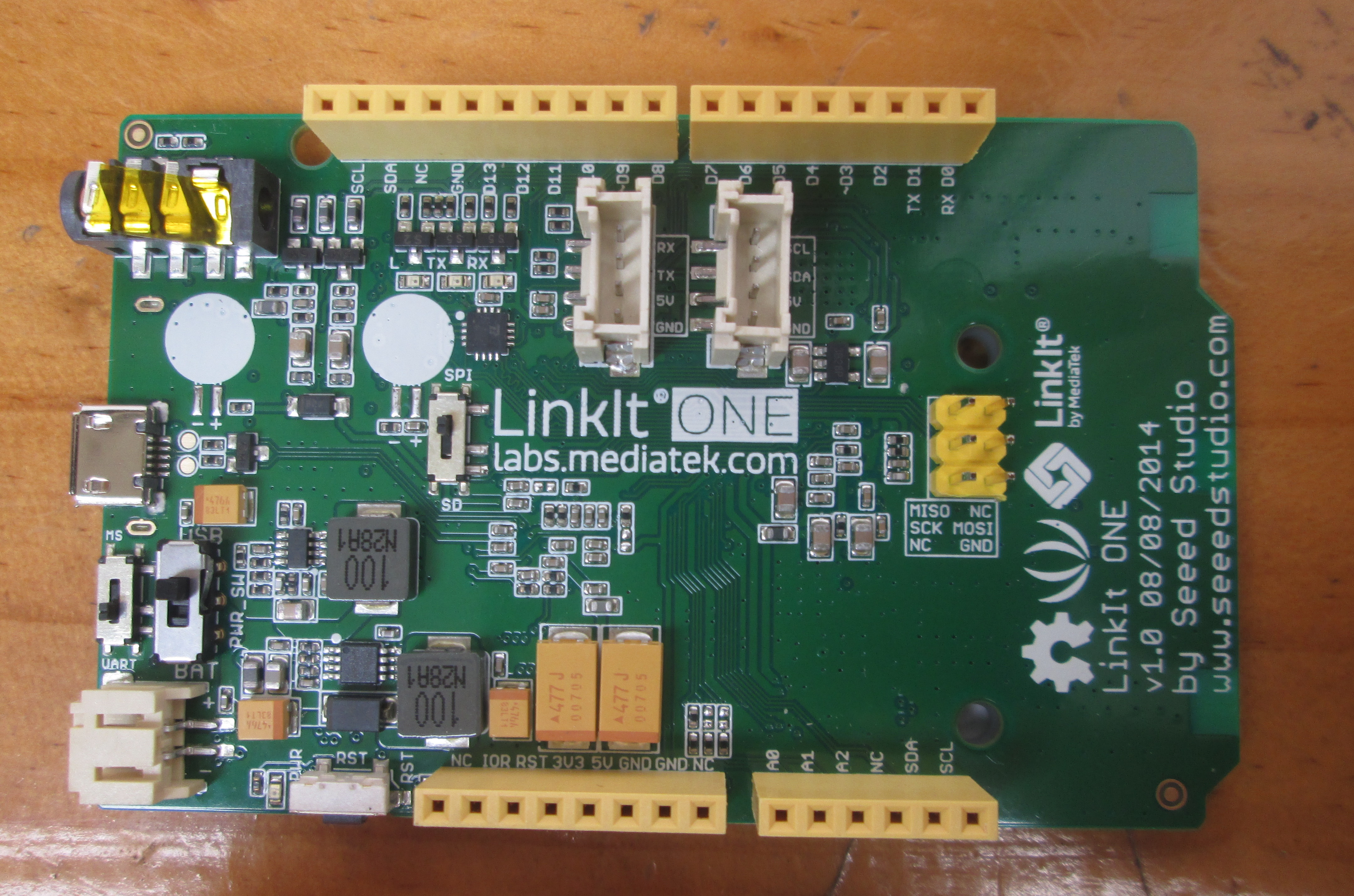
