Joining component in schematic problem

I’m trying to learn schematics. I’ve got my project breadboarded and am now trying to document the project with a schematic. At early stages of learning this and can’t get led components to attach to the power wire. And on the ones that do connect (green lines), one has a large connection point, anaother small, and another none at all. I don’t understand.

here’s the breadboard,

And early stage schematic (I know some dotted lines are not yet connected to the right places.)

I can’t find any tutorials that help me. Any help or pointing to some books or articles for a beginner are much appreciated.

thanks,

hal

Your best bet is to upload the sketch (the .fzz file, upload is 7th icon from the left in the reply menu) so we have the sketch to work on. It looks like (because of no rats nest lines to the anodes of the LEDs) that you don’t have connections to them in breadboard. If you right click on a pin in breadboard view Fritzing will light all connections yellow like this. You will likely find the leds in breadboard don’t all light up yellow.

Here I right clicked on the bus strip at the green arrow and all connections light yellow. I think there are tutorials on the main site in the learning section (it has been 8 or 9 years since I started in Fritzing so I don’t remember any more :slight_smile: .)

Peter

Having the sketch file @vanepp mentioned would make it easy to confirm, but I expect that you placed wires from the leds to the red ‘power bus’ wire. That does not actually connect the wires. Wires only connect at the ends (think of them as insulated). To get what you want, place “U” shaped wires from each LED to the next, then from the pin of one LED back to the breadboard. positioning the wires so that they are top of each other makes it look the same as you have now.

The rats nest (dotted) wire on breadboard from occupancy switch to nano, is because you have connect the opposite pin of the switch in schematic view. A switch does not normally have polarity, but Fritzing knows which pin has been connected. Reverse the pins on one of the views.

@vanepp and @microMerlin,

Okay. Here is the sketch. Left clicking on the breadboard does light everything up yellow.

Nano Seat Occupancy.fzz (32.6 KB)

Thanks for the U shaped wire strategy. I’ll give that a go and see what happens.

And also thanks for the tip on the “non-polarized, polarized” explanation. That too, I’ll give a try.

In the meantime, what’s the purpse of “rats nest” lines? Trying to remember last nights efforts, I seem to remember if I deleted the dotted l in schematic, something unwanted happened on the breadboard (maybe component deleted?). Thank God for ctrl-Z.

hal

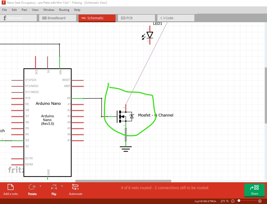
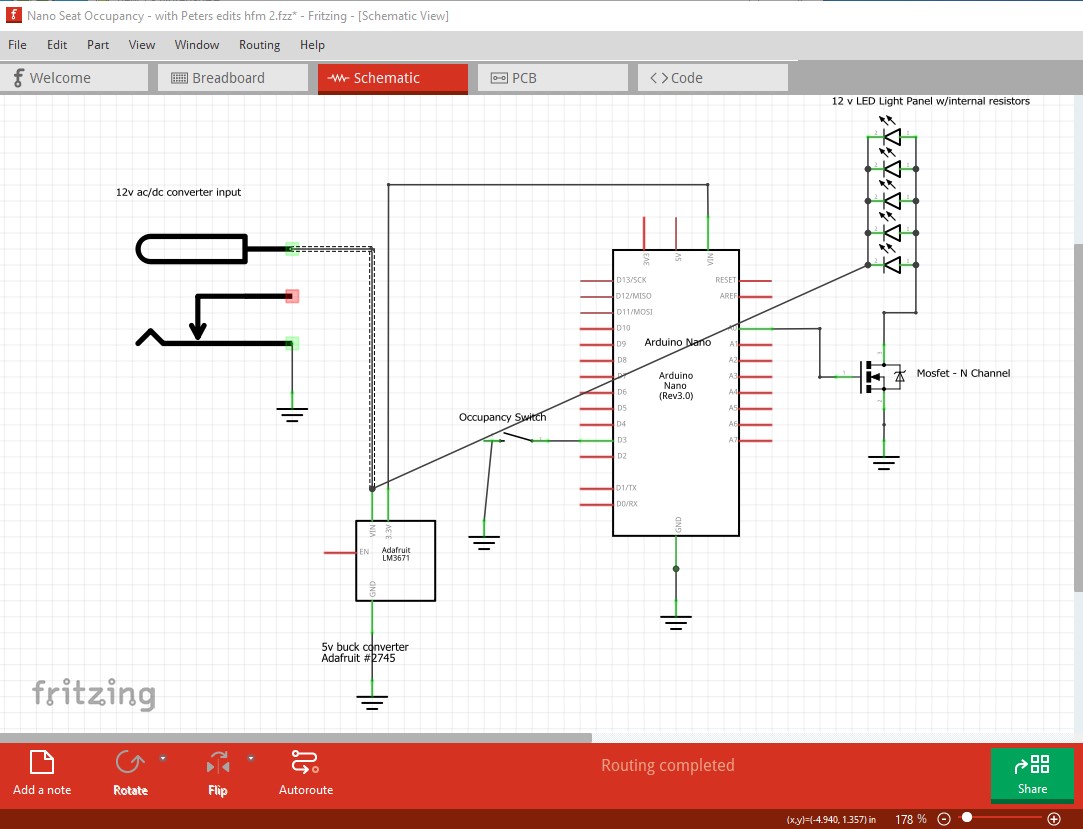
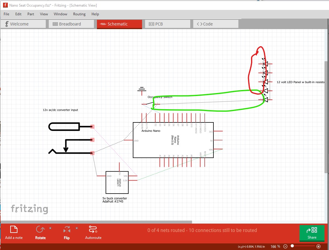
OK a fair number of problems here (not all of them that I understand how they were created!) I started in schematic and selected all traces then hit delete to delete them all.

capture

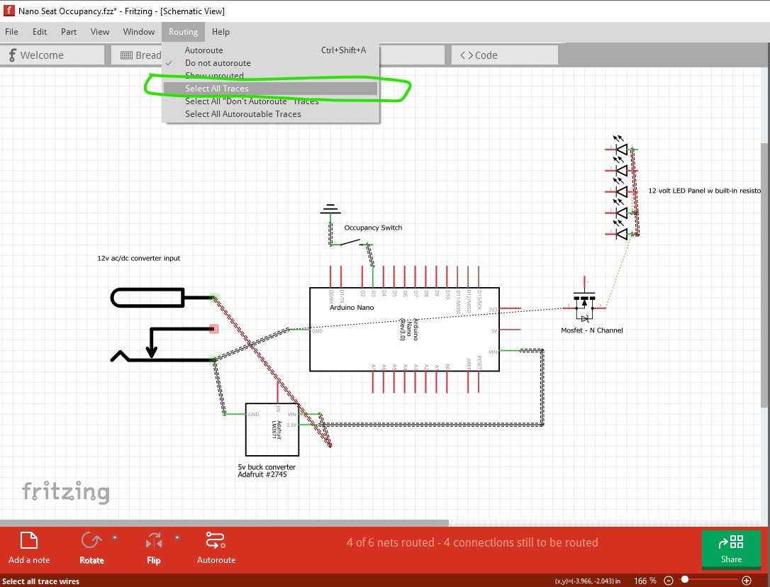
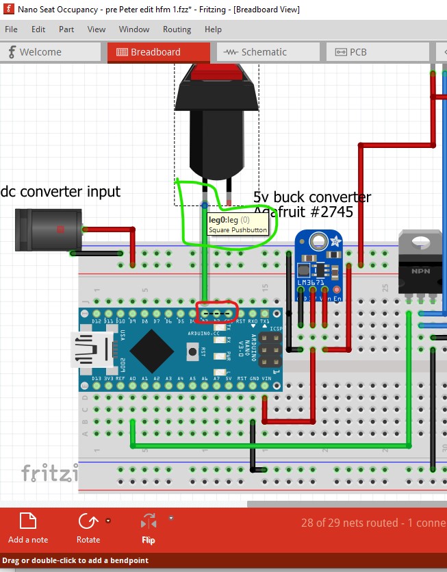
that shows us all connections that Fritzing thinks are in breadboard. As we see a lot of them are missing (circled in red!) indicating breadboard isn’t correct. Note that connections you make here or in pcb will reflect as a connection in to the other two views (and if they are incorrect can cause shorts!)

capture1

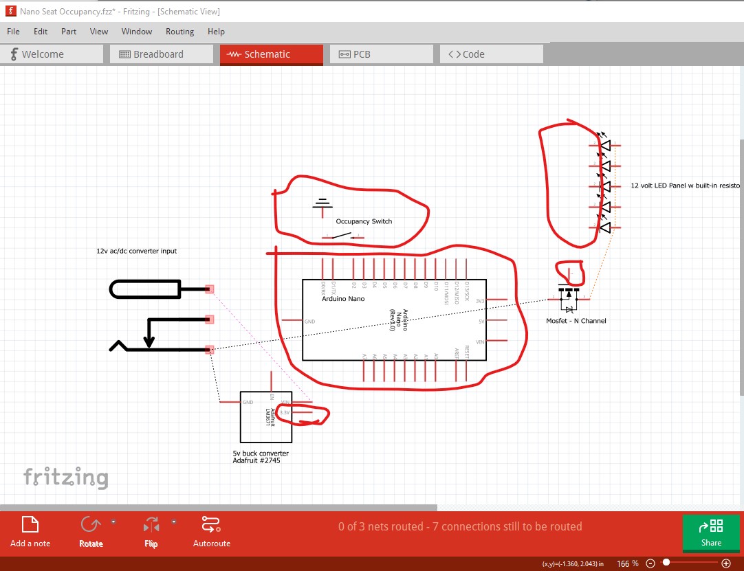
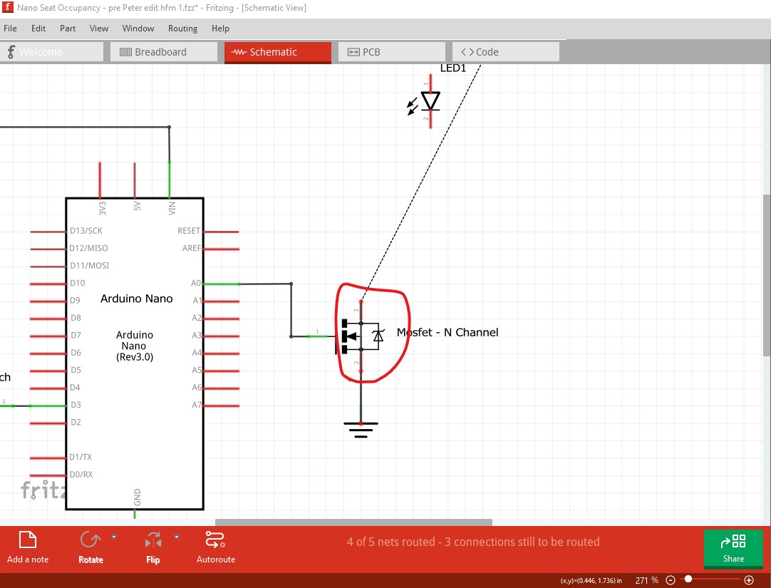
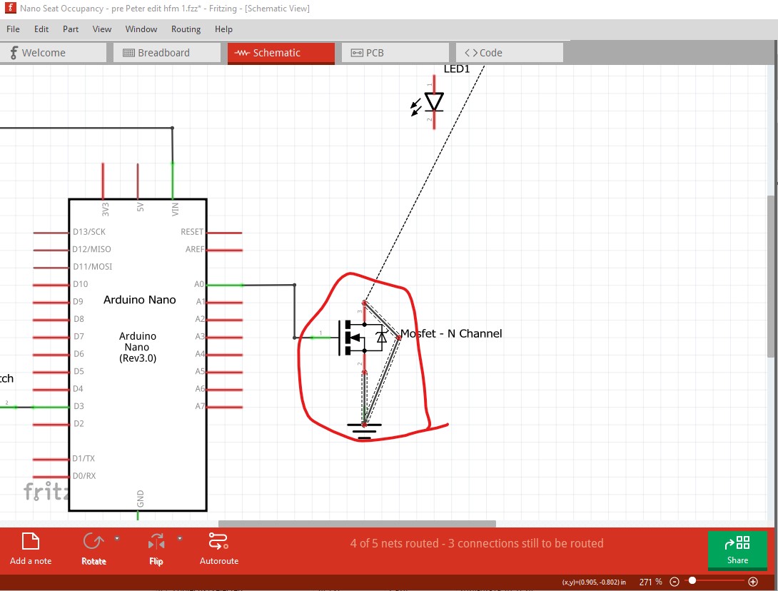
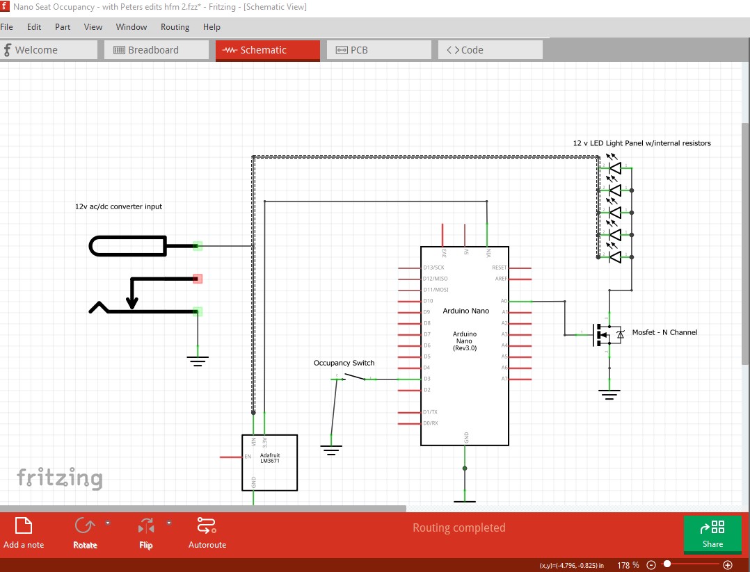
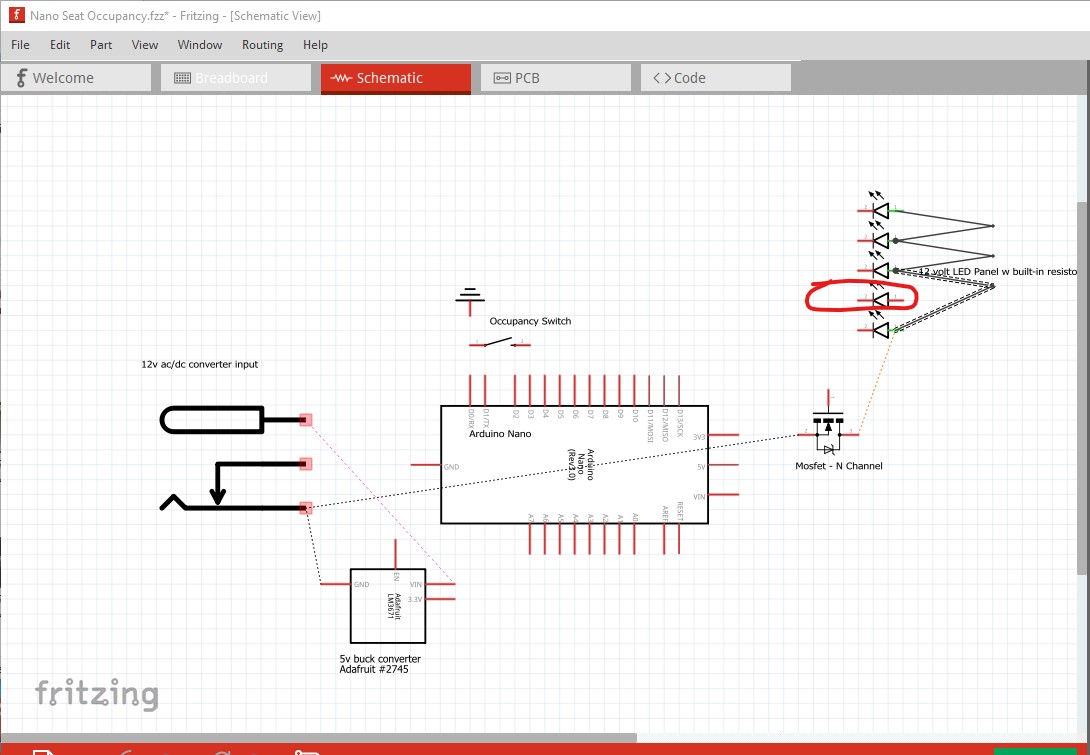
here I connected the rats nest lines reflected from breadboard. We see (the red circle) one LED cathode has no connection. Then I deleted all traces again (not required but neater.)

capture2

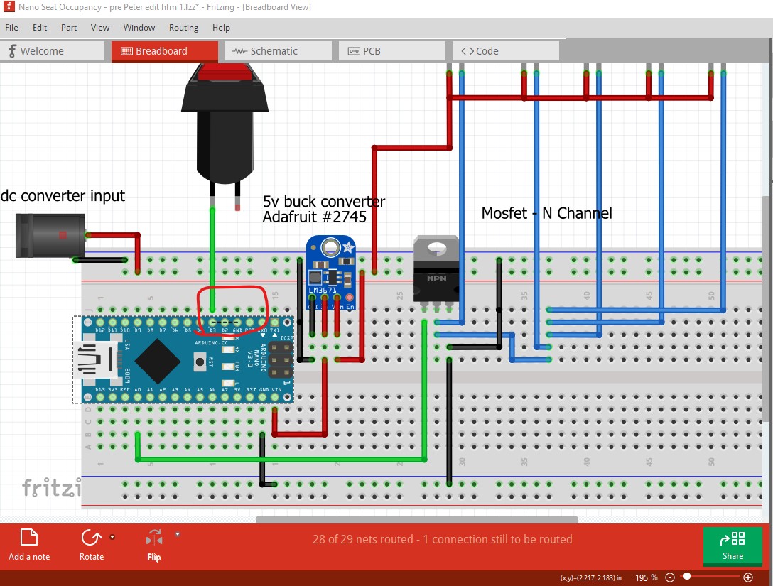
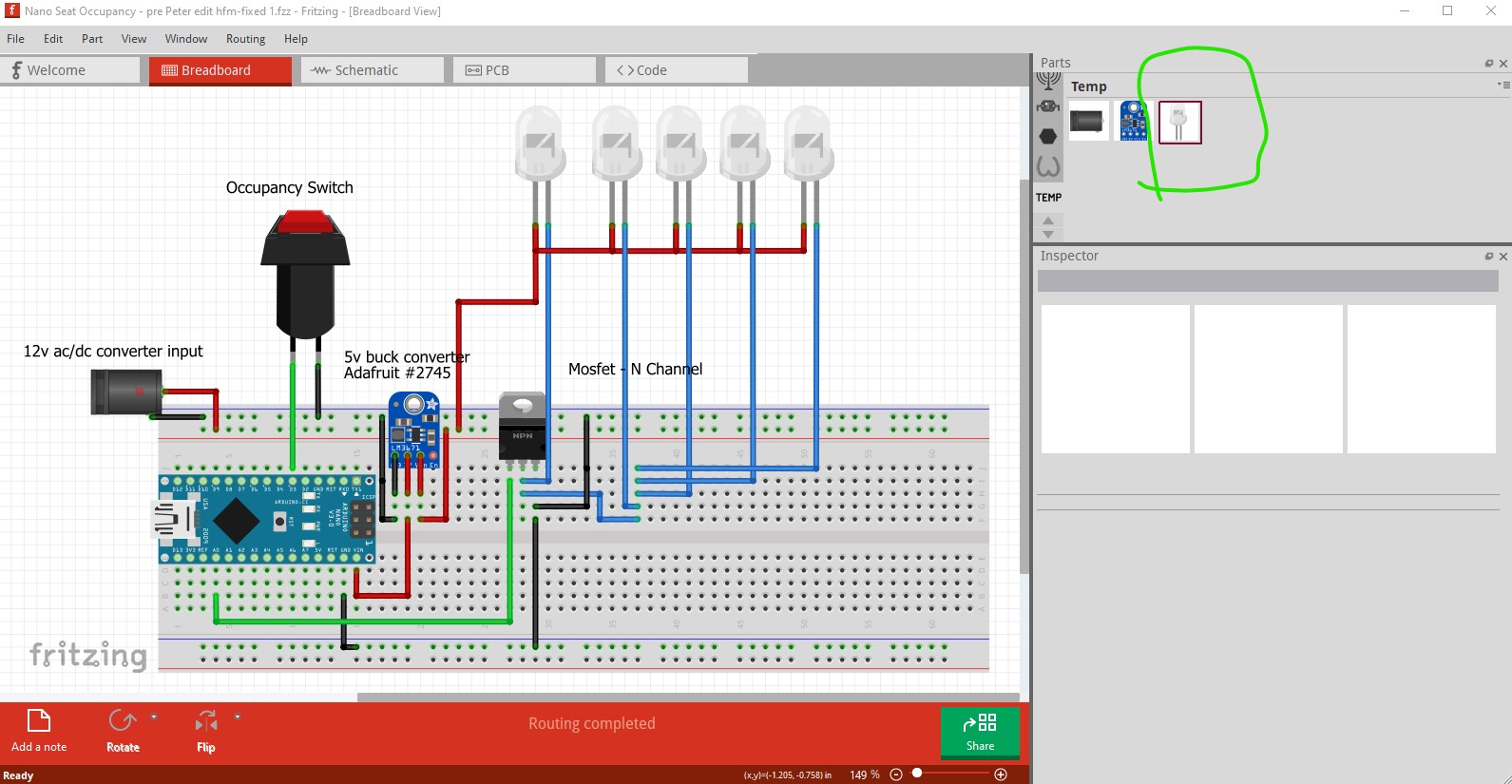
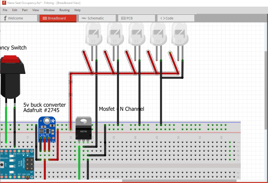
now switch to breadboard (with no connections in schematic to reflect here.) The first thing is the nano is not correctly seated all the pads should be green indicating a connection to the breadboard

capture3

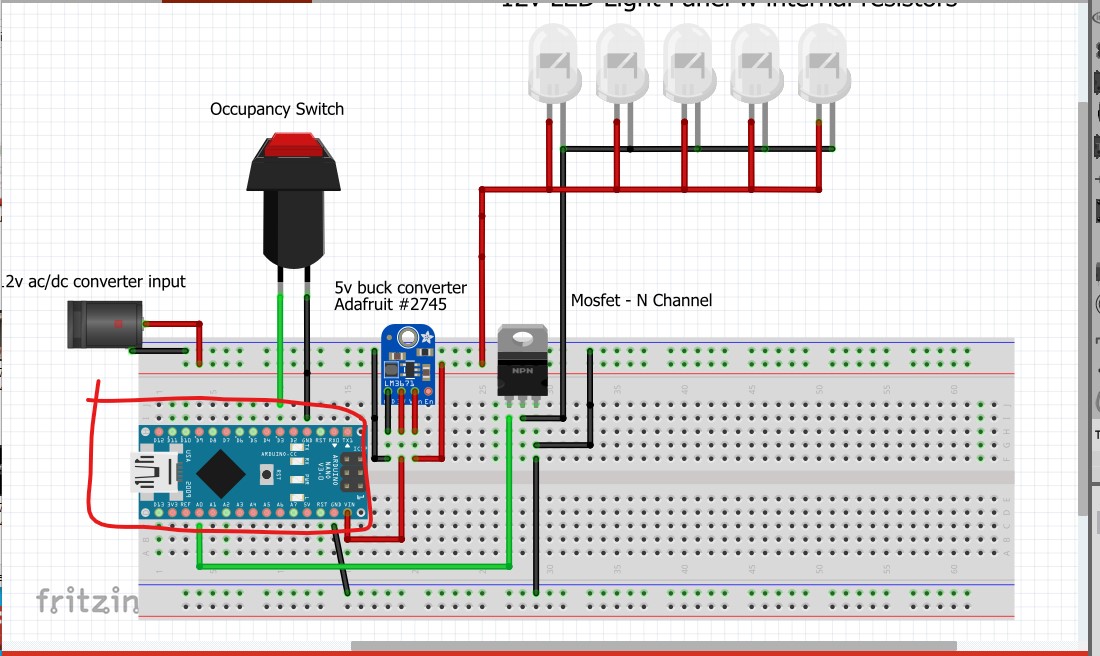
so move the nano up then down to make that happen.

capture4

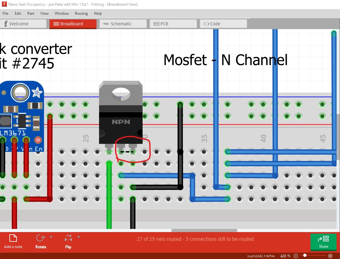
then right click on the gate of the mosfet and we see there is

capture5

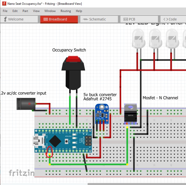
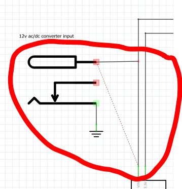
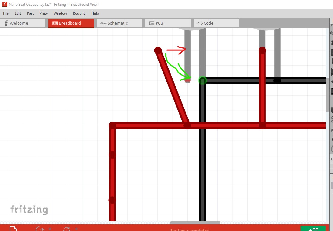
we see (circled in red) that the connection to the nano is not yellow (and thus not connected) so move the wire on the breadboard to get it to connect.

capture6

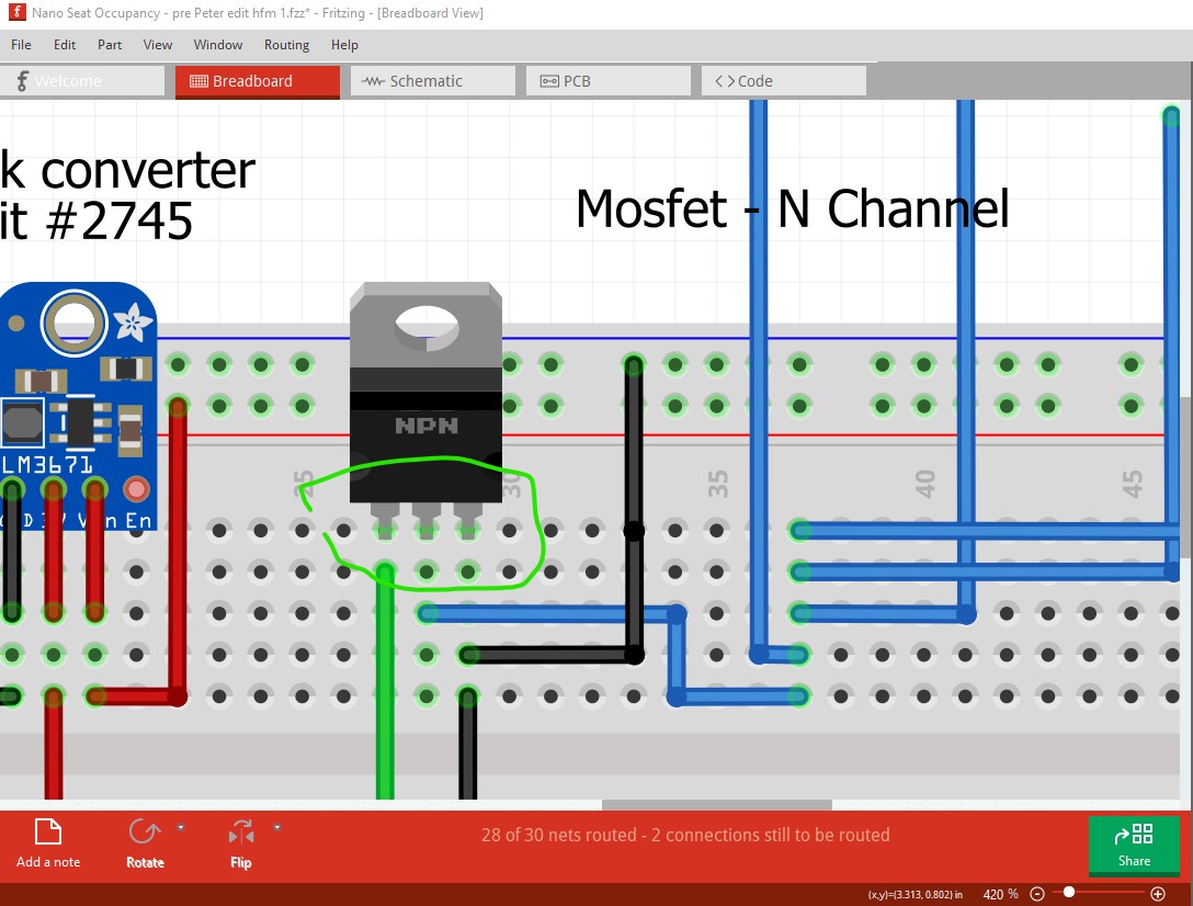
No everything lights up yellow as it should. Same with the ground wire to the nano, no connection to the nano

capture7

so move the wire to create one (moving a wire will cause a connection to occur if it is over a connection point such as the breadboard!)

capture8

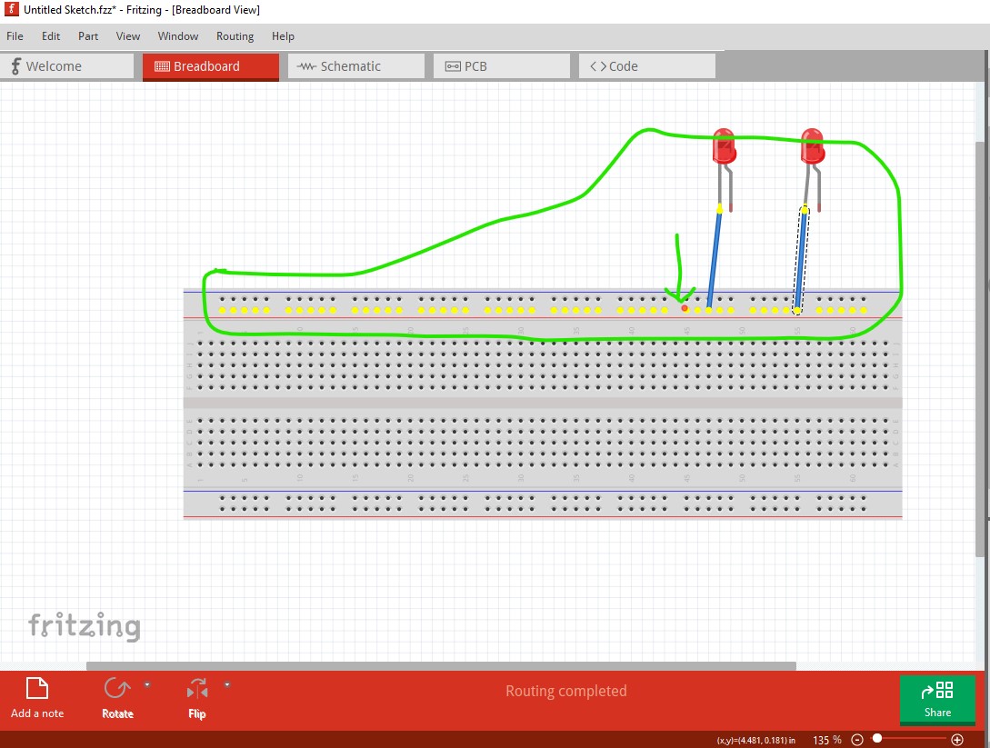
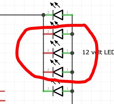
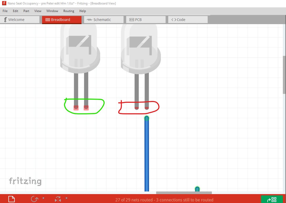
now we see the ground wire to the LEDs is one pin too far to the left

capture9

so move it one pin right to get it to connect.

capture10

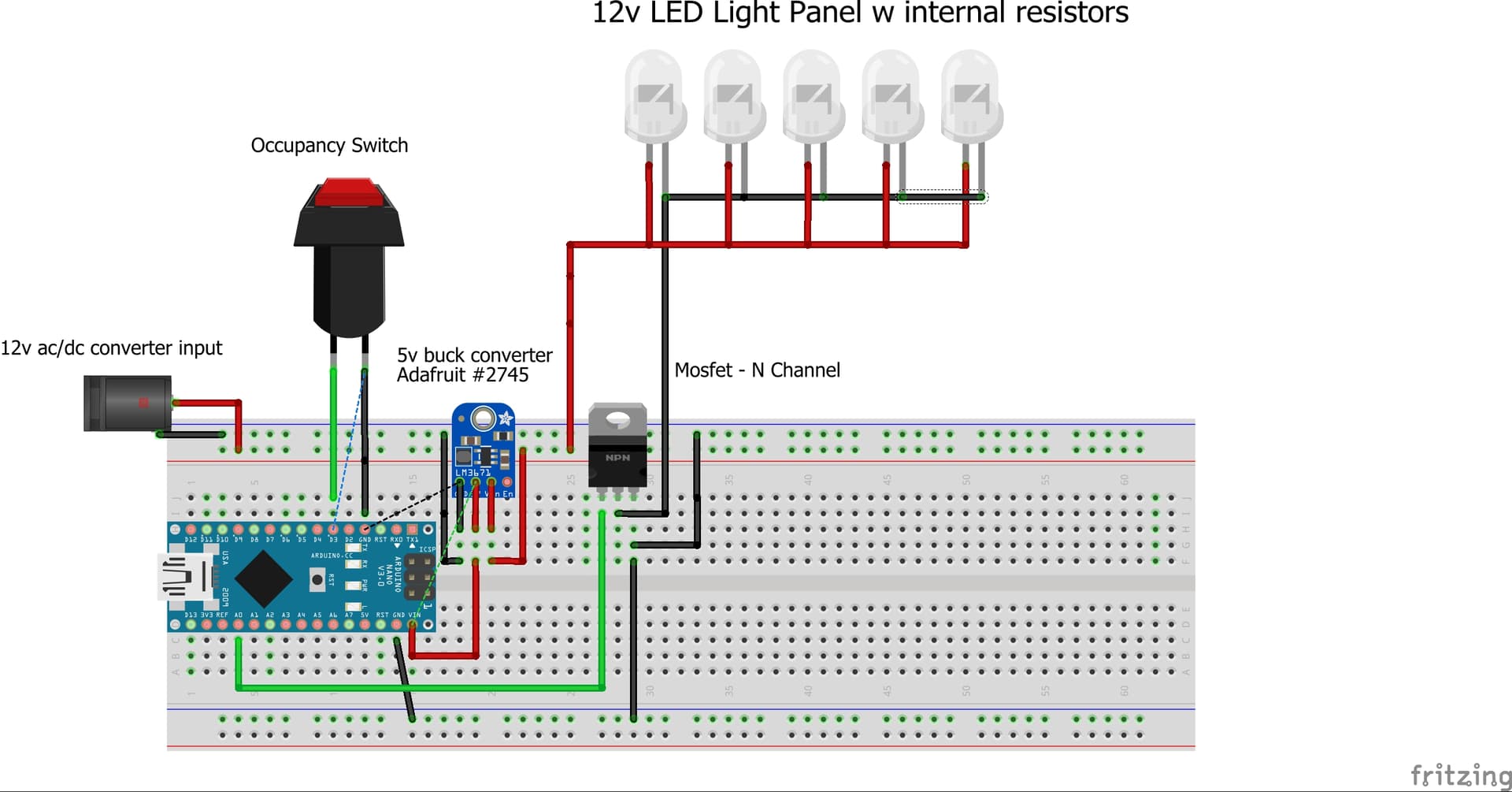
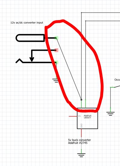
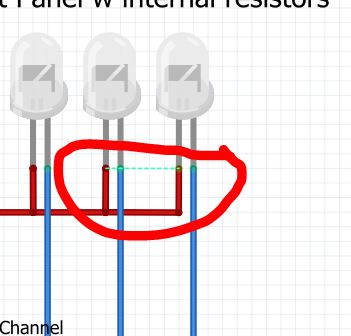
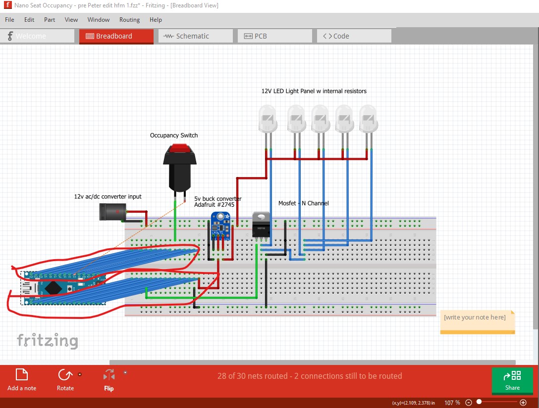
The 12V connection to the LEDS looks fine but isn’t.

capture11

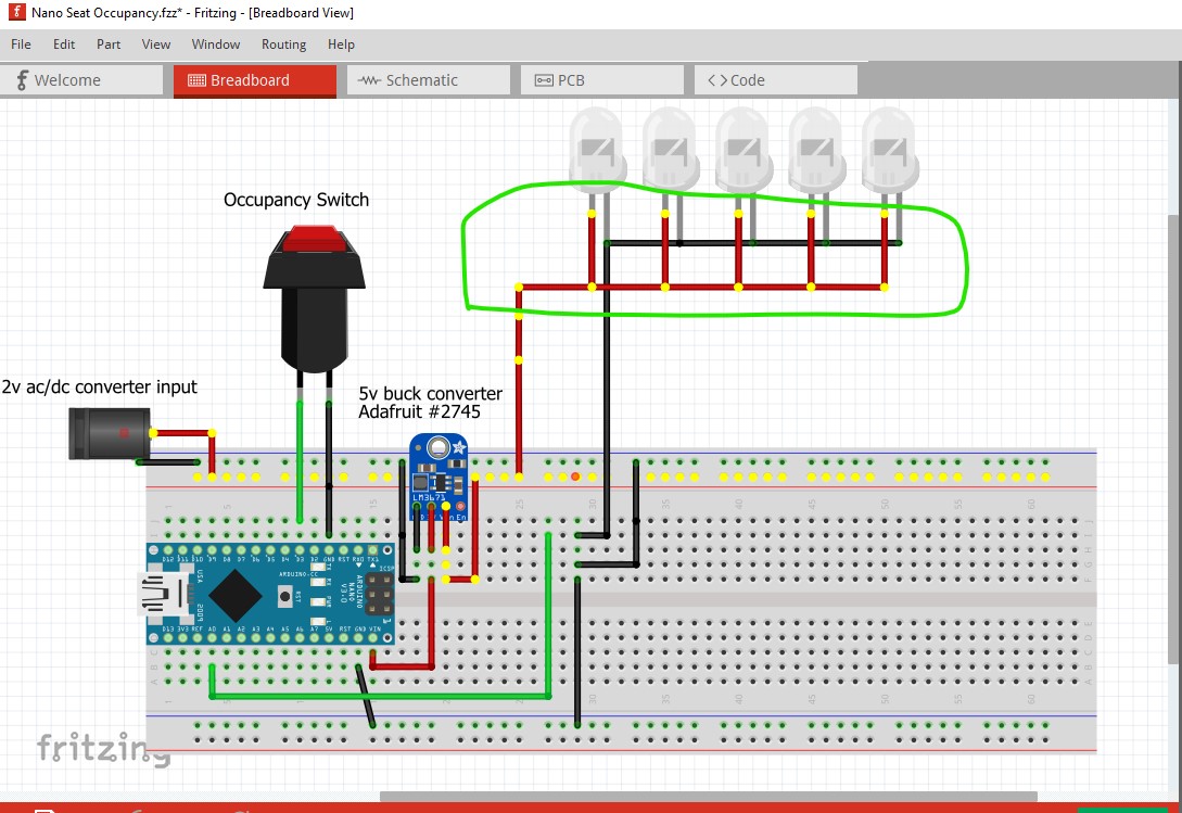
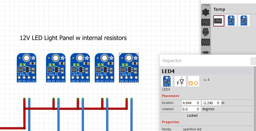
because the LEDS are bendable legs, the entire pin (unlike normal) isn’t part of the connection. Only the red dot on the end is the connector (the green arrow) where the wire was connected will not make a connection to the LED.

capture12

so move it so it connects then switch to schematic to make sure the connection actually occurred indicated by the rats nest line.

capture13

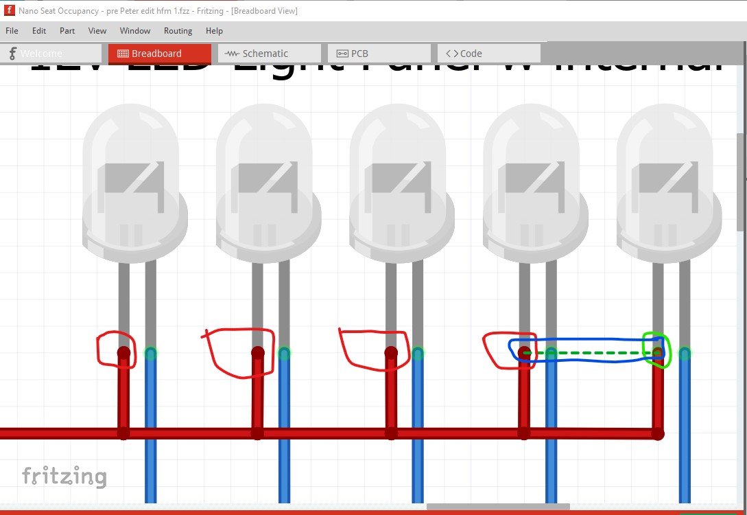
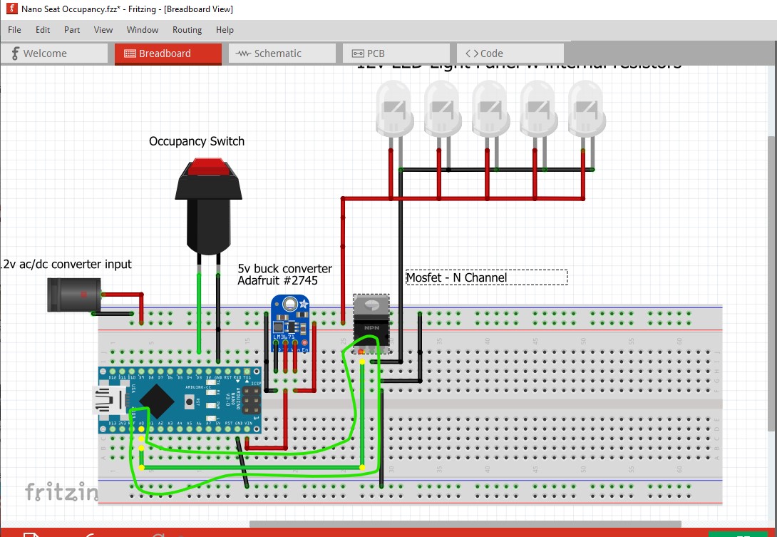
back in breadboard I dragged the black wires on the LEDs apart. This is one of the things that I don’t know how you did. The section circled in red is wrong.

capture14

so I deleted the wire and rewired it correctly by connecting them to the ground bus on the breadboard (I would probably move the LEDs on to the breadboard but didn’t in this case.)

capture15

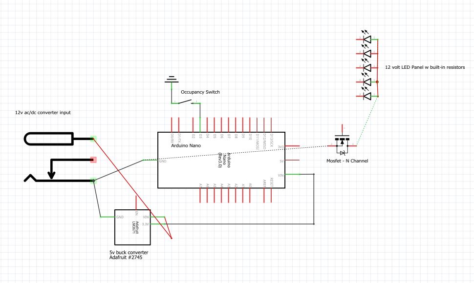
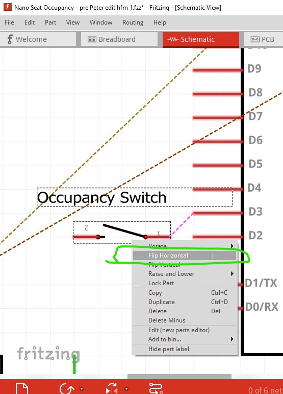
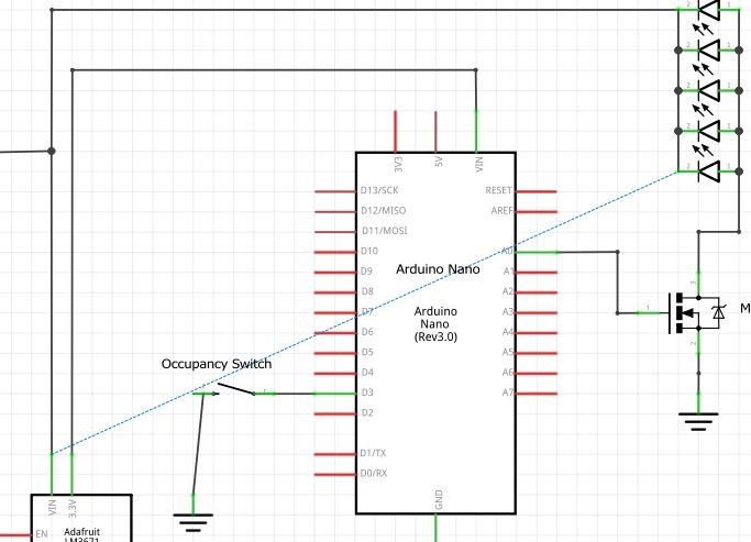
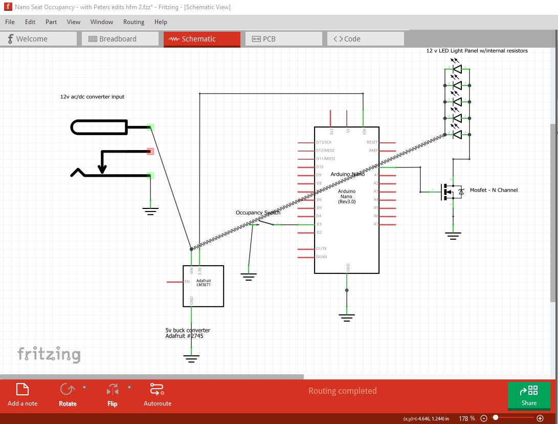
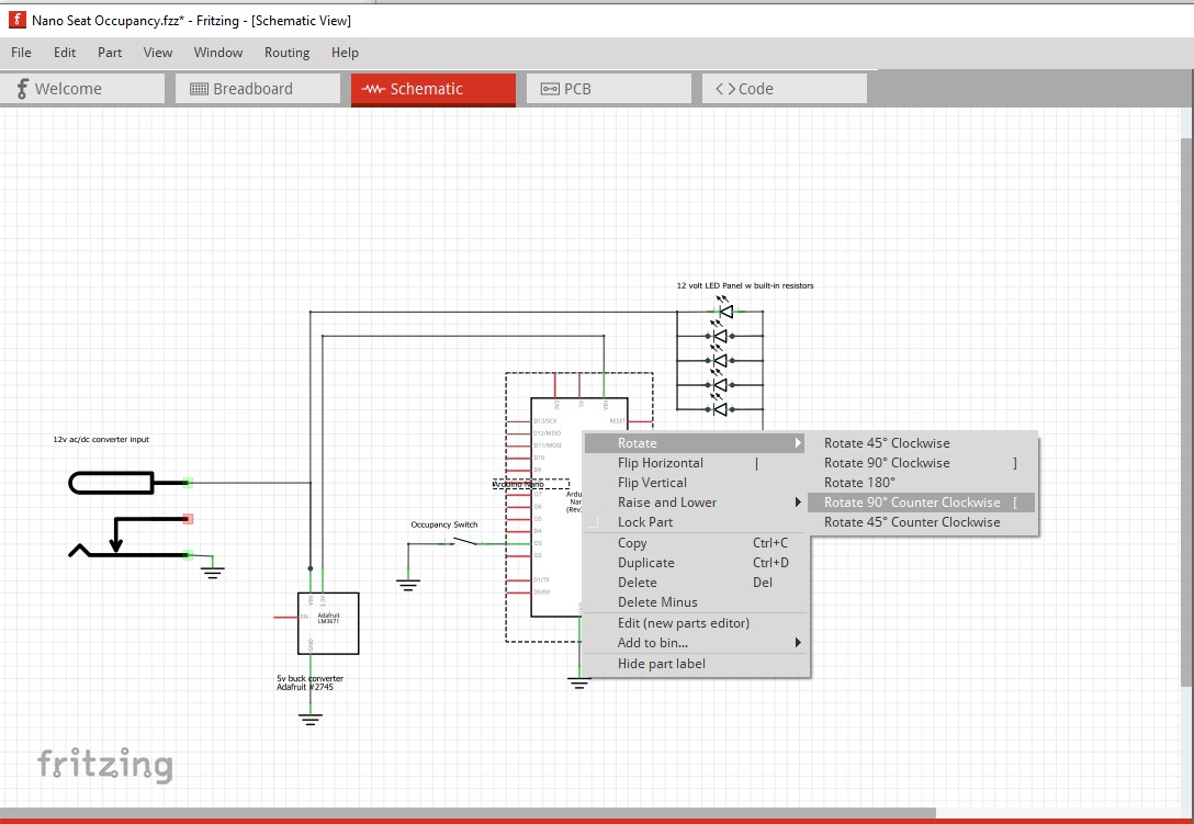
switching to schematic I rotated various parts (the nano in this case) to align them better by right clicking on the part and selecting rotate.

capture16

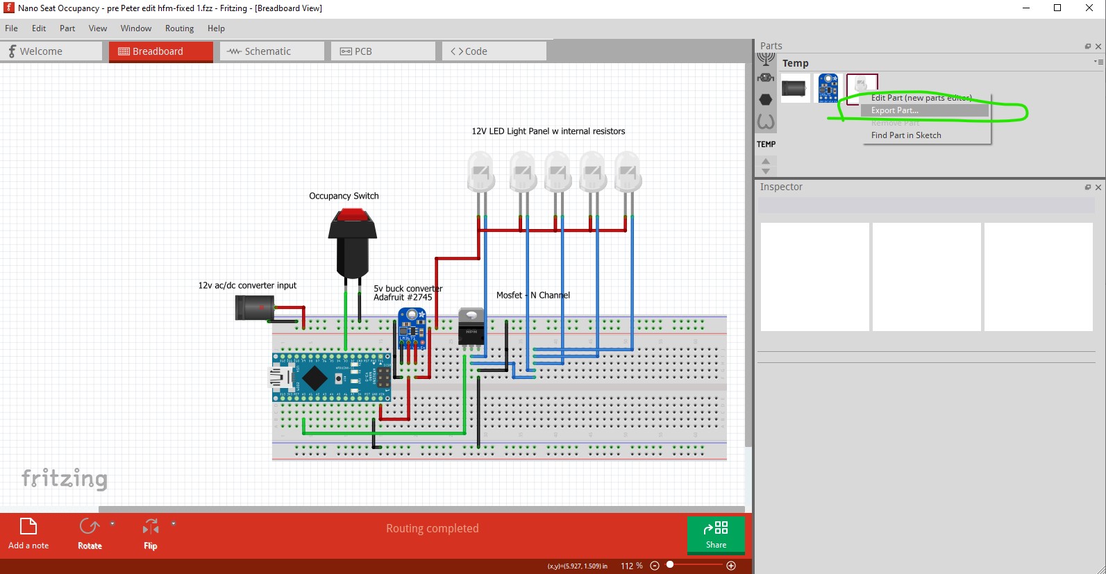
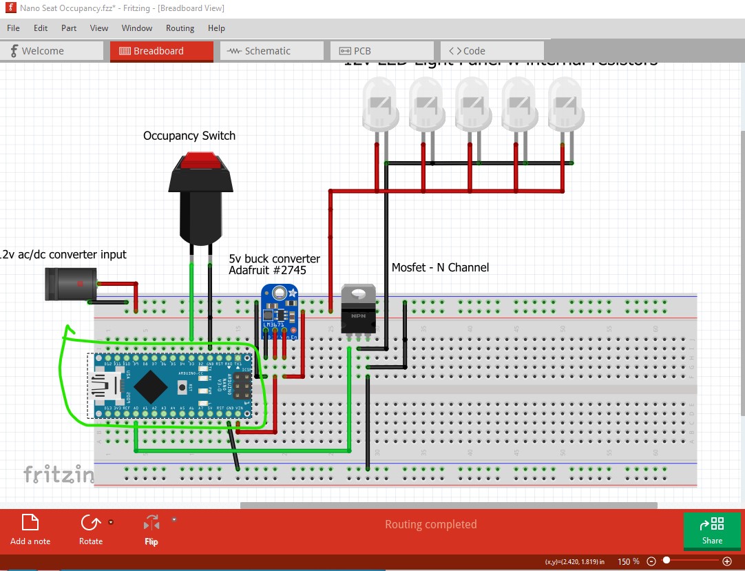
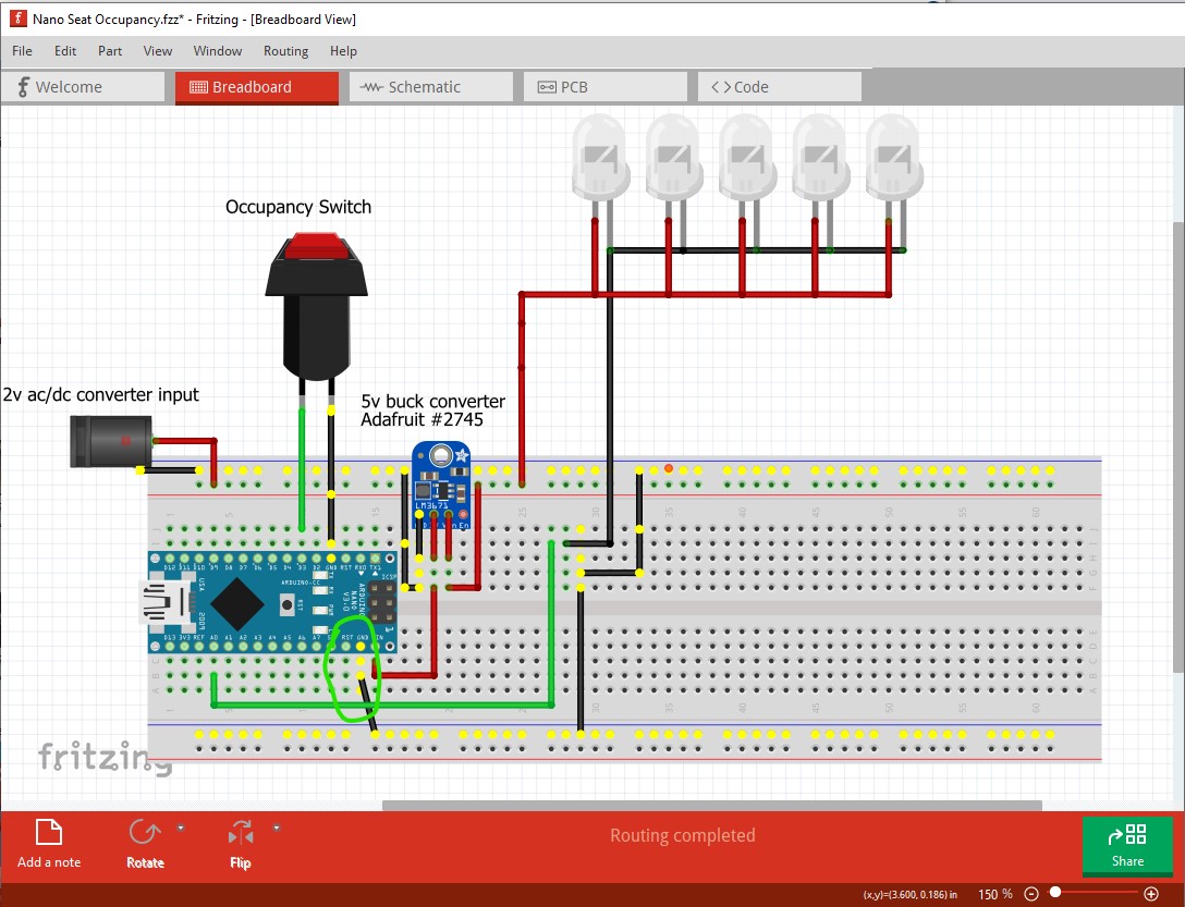
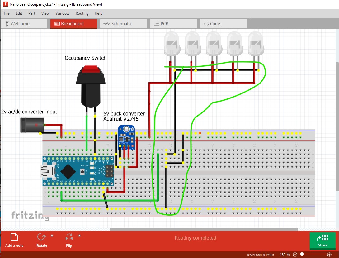
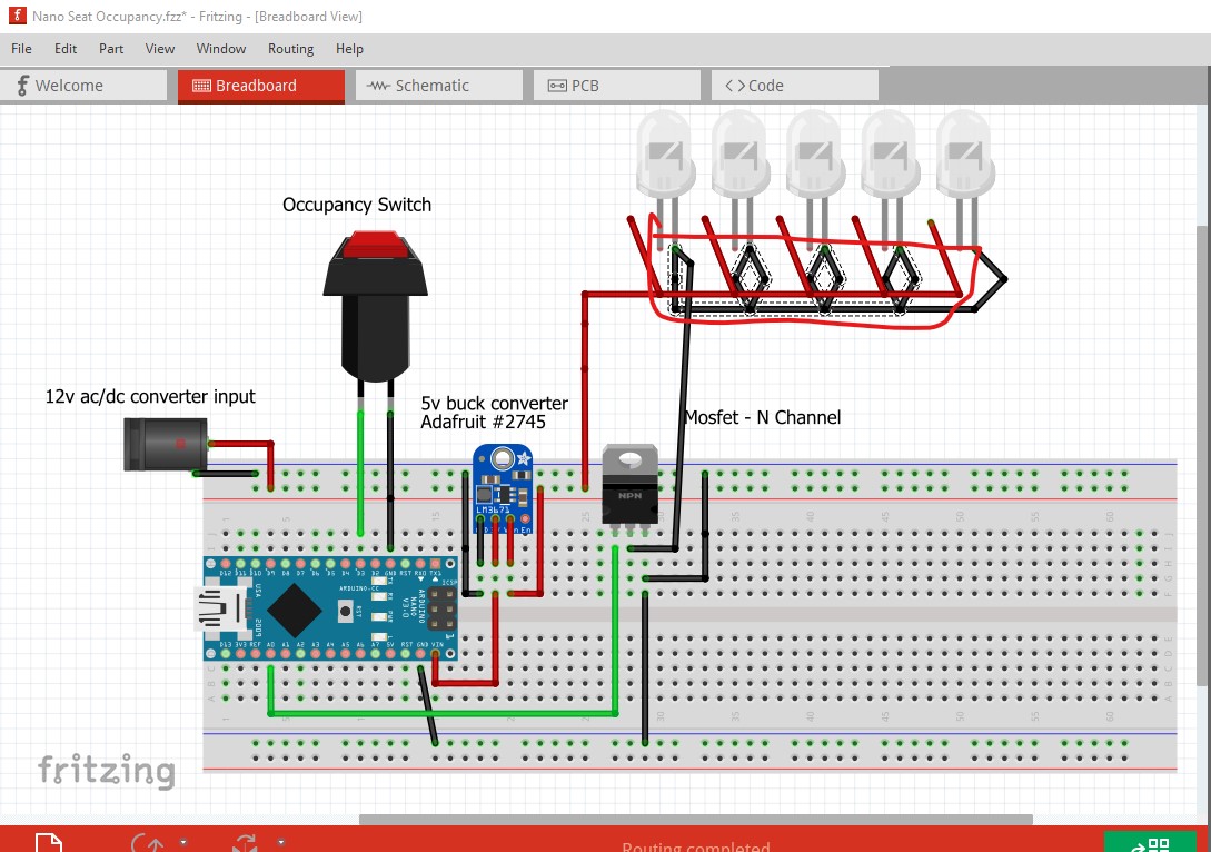
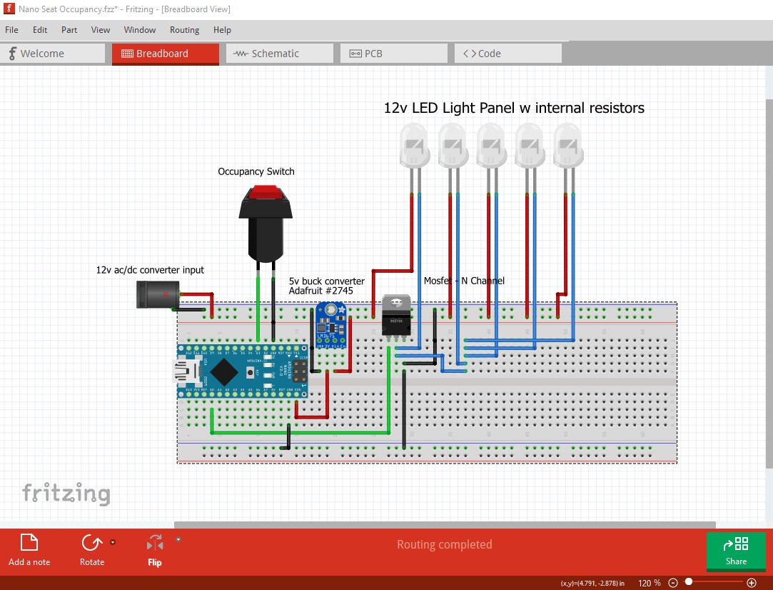
That creates this breadboard where routing complete is at the bottom of the window

capture17

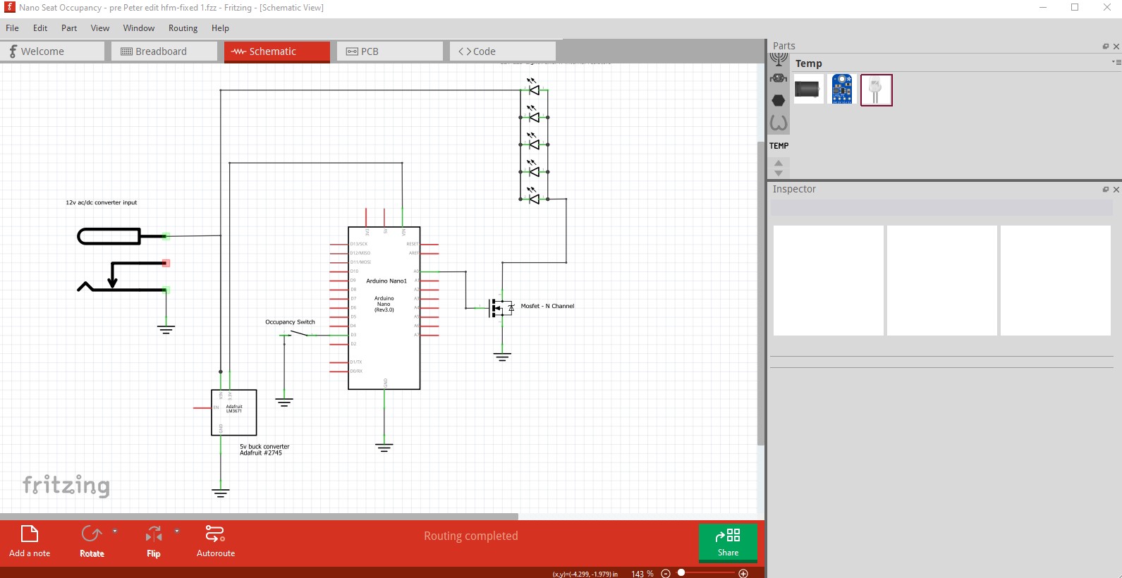
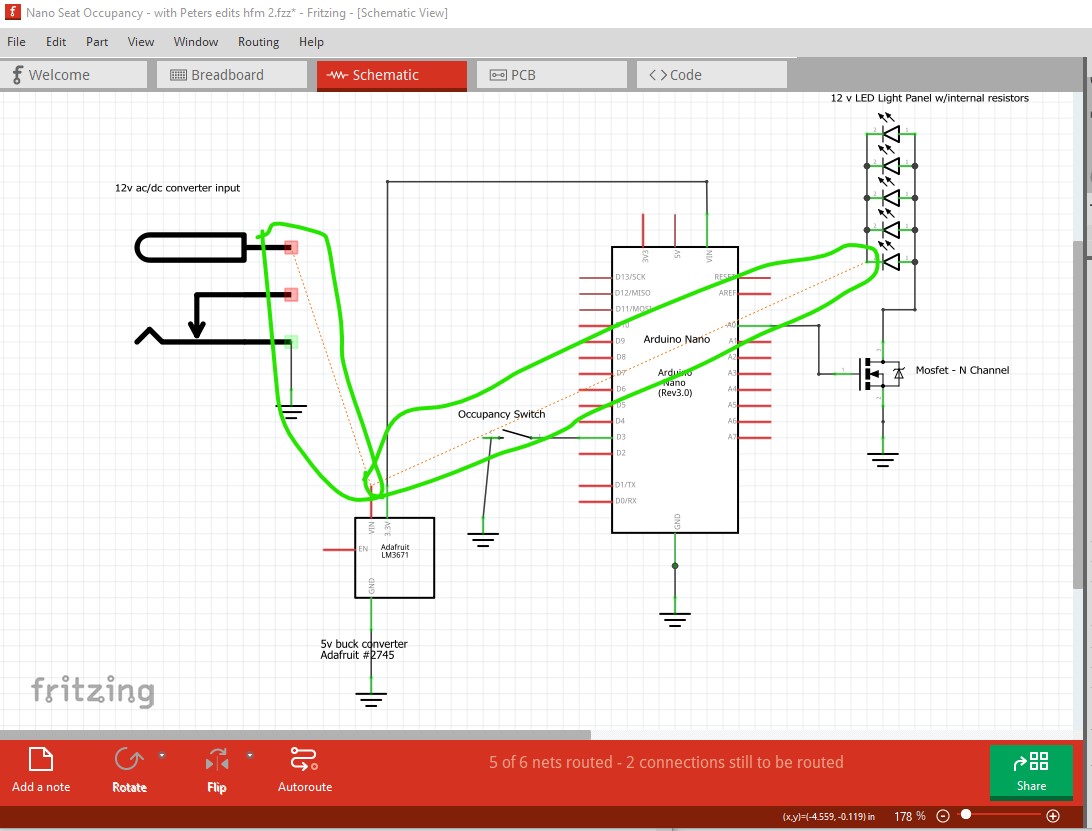
and this schematic also with routing complete at the bottom of the window.

capture18

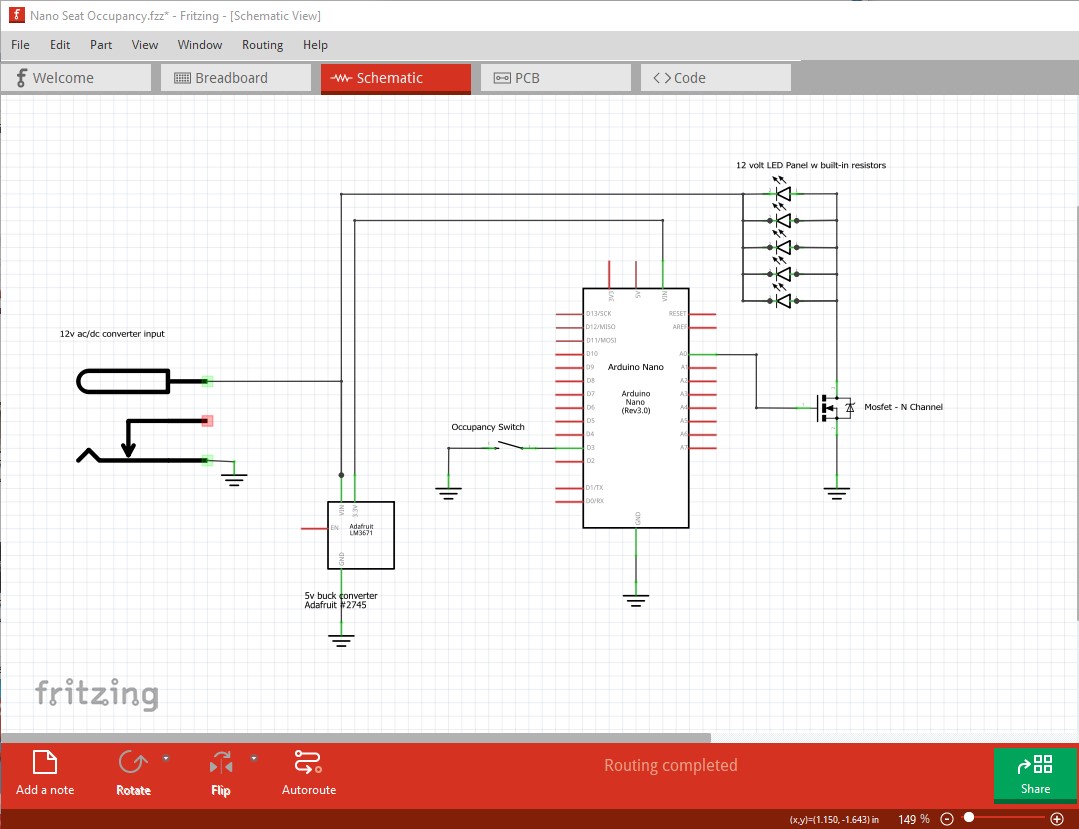
which is how I would do schematic. All these changes are in this sketch

Nano Seat Occupancy-fixed.fzz (36.6 KB)

which you can download to look over and change as you like. If something isn’t clear feel free to ask.

Peter

1 Like

Wow Peter @vanepp,

I so appreciate you taking the time to so thoroughly examine, explain, and fix all those problems. What you’ve put together seems like a superb textbook on working with the breadboard and schematics in Fritzing.

I’ll take my time to work on each point that you’ve graciously explained and documented.

Back to you later with questions as I work through this.

Thank you,

hal

So, so helpful Peter - thanks. Pretty darn cool how you moved and ajusted components to make it visually more understandable. And your diagrams were a big help.

A few problems I ran into.

*On schematic when I try to move connection point on wire from 12v input to intersect with the buck converter wire it loses connection.
Good connection

Not connected when wire moved to different intersect point.
12 volt not connected

Also I can’t get 3 of the leds to connect.
leds not connected to 12v

There’s a rats nest on the breadboard between to the two right leds. What does that mean?
led bb rat nest

Here’s my updated sketch per your guidance. What am I doing wrong in regards to the above items?
Nano Seat Occupancy - pre Peter edit hfm 1.fzz (38.1 KB)

Some observations and questions I wrote down perhaps you can comment on.

    1. when you said “reflected from breadboard”? what does reflected mean?
    1. So interesting that even though on the breadboard, it looks like there are connections, but as you point out, the yellow doesn’t light up on the nano.
    1. Strange to me that moving components on the schematic, doesn’t move them on the breadboard.
    1. Interesting how clicking on ground symbol connection in schematic lights up all the grounds even though they aren’t shown as wired together. Smart symbol I guess.

Thanks Peter,

hal

It appears there is something incorrect in the LED part you used which looks to be causing issues. I grabbed a copy of the part and corrected it and that looks to have fixed things. Here is a what I changed (which will likely answer your questions as well as some of the errors in the sketch illustrate the issues.) In this image only the right most connection (circled in green) is actually connected. The rats nest line between it and the next LED indicates a connection in schematic that isn’t present in breadboard. Note the red wire (circled in red here) doesn’t have a green square indicating a connection unlike the rightmost LED. I think that may be a problem with the part and why I replaced it.

The LED on the left is my replacement (with a bigger contact area although that shouldn’t matter) compared to the original LED on the right (with the wire moved for clarity.)

next there is a short (indicated by the rats nest line from schematic) between the source and drain of the mosfet.

that is caused by this wire in schematic (which then reflects in to breadboard and pcb)

that is caused by the bottom ground wire running too far up and shorting the source to the drain.

deleting that wire fixes the problem

which also removes the rats nest line from breadboard.

here I dragged the nano out from breadboard. It has wires connected to breadboard (probably because it got moved and breadboard will add wires to the existing connections.)

This shouldn’t hurt anything but I chose to delete the nano and move a new copy on to the breadboard

doing that indicates a short (again from schematic) from D3 to GND. This one is caused by using the wrong pin in schematic. Here I right clicked on the pin of the switch with the wire connected to it. That indicates this is leg0 of the push button.

switching to schematic we see that the leg1 of the push button should be going to ground and leg0 should go to D3. To fix this I flipped the push button in horizontal in schematic which orients it correctly.

Then connecting the ground in breadboard completes the routing. If you look in the temp parts bin (with the sketch below loaded!) and right click on the new LED and select export part it will write a .fzpz file for the new LED part to the file system so you can use it later.

and schematic as well.

and the sketch that implements all of this.

Nano Seat Occupancy - pre Peter edit hfm-fixed 1.fzz (40.7 KB)

As we saw on the switch, a wire in schematic or pcb will reflect as a rats nest line in to the other 2 views and if you get the orientation incorrect can cause a short in another view.

the scheme isn’t perfect. It lights the end of the wire in yellow even if it is not actually connected to anything. You need to check that the connection you expect is green (connected) rather than red (unconnected) to be sure the connection has been made. With smaller pins as in the LED part that can be difficult!

Fritzing has no idea of how things are arranged (other than connections via the rats nest lines) between views and thus can’t move parts in the other views except by you going to the view and moving them.

All the grounds are in the same net, the ground symbol and the power symbols ate attached to that net and thus light yellow when that net is selected. Hope this helps!

Peter

1 Like

Wow Peter,

This is incredibly helpful. That obviously took a lot of time to troubleshoot. Thank you so much for the marvelous explanation and documentation as to the problems I ran into.

Debugging the LED pins was true detective work. Again thank you for taking the time to do that. And creating a new one that works correctly is way beyond.

I’m going to download your corrected sketch as a comparison against reworking my sketch. Hopefully I won’t run into any more puzzlements that cause me to come seeking more of your time.

THANK YOU!

hal

Hi Peter,

I loaded your sketch to get the fixed LED part and got buck converter images on the breadboard where the LEDs go. In pars Inspector it looks like the schematic symbol is right, just the bb image is wrong. Is it hard to fix?

thanks,

hal

That is odd. For me it loads the LEEDs

with the new LED in the temp parts bin (from th .fzz file I uploaded!)

In any case here is the new LED part so you can try it in a sketch.

LEDs.fzpz (5.0 KB)

Peter

1 Like

thanks Peter,

I just knew it couldn’t be right. I tried to load the new part but it says that part already exists. So I’m trying to delete the wrong one but no luck there either.

I’m using Fritzing version 0.9.3. I wondered if that could that have anything to do with it? So I just downloaded the latest 1.0.2 and no difference. Geesh.

hal

@Vanepp,

Got it working Peter. Don’t know why this fixed it all but here’s what I did.

  1. updated to current Fritzing version
  2. opened my prior defective sketch,
    2a) your new LED was now in the Temp folder
  3. opened my prior defective sketch, deleted my LEDs and replaced with yours.
  4. opened your sketch and all the LEDs were properly displayed.

Go figure?

Now on to reworking my sketch to match yours.

thanks,

hal

@vanepp ,

One last item Peter. I can’t resolv the rats nest on the schematic from the buck converter to the LEDs. I think all connections on the bb and schematic are green but yet the ratsnest persists.

buck converter rats nest schematic

Here’s my sketch reworked to match yours. (However, for the life of me I couldn’t get the positive power to connect to all the LEDs without individually wiring each one separately to the bus.

Nano Seat Occupancy - with Peters edits hfm 2.fzz (40.2 KB)

Apparently there’s one final thing I’m not getting right.

thanks,

hal

There are two wires there (here I deleted the wire to the LEDs to show the two rats nest lines)

So you need to create two lines and then drag them to overlap to complete the connection like this.

the wires are all separate but overlaid on one another for appearance.

Peter

1 Like

Super clear and efficient! Much thanks Peter. I think that does it.

hal