Hi,
I needed an N-Channel JFET and since there’s no JFETs in Fritzing’s part library I decided to create one.
At this point I thought: Hey, why not do a P-Channel just for completeness’ sake.
So I did.
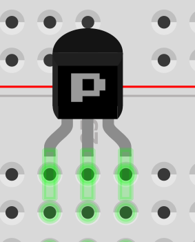
I’ve modelled the N-Channel after the BF245 (GSD pin configuration) since that’s what I needed, and the P-Channel after an NTE489 (DGS pin configuration) since that’s the first I found when searching around.
If someone needs a different pin configuration or package just write a reply or send me a message and I’ll see what I can do.
Hi there, thanks for the feedback!
Yep, I made lots of mistakes for the pin assignments.
I’ve corrected them, check the new downloads.
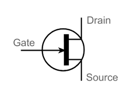
As for the labels in the schematic view, I’ve followed the way other transistors are done in Fritzing which is to label the pin numbers. If you hover over the pin you will see the names.
Hello,
Yes they are okay now…
I just replaced breadboard “terminal” to “leg” Id in part file… Now you can use them as bendable legs…
Here… (don’t know about the macOS part) JFET_N_GSD_BF245.fzpz (6.9 KB) JFET_P_DGS_NTE489.fzpz (7.0 KB)
Indeed welcome aboard! People making parts are especially welcome , that said here is my cut on this (which started with the original .fzpz files so is now somewhat out of date) :
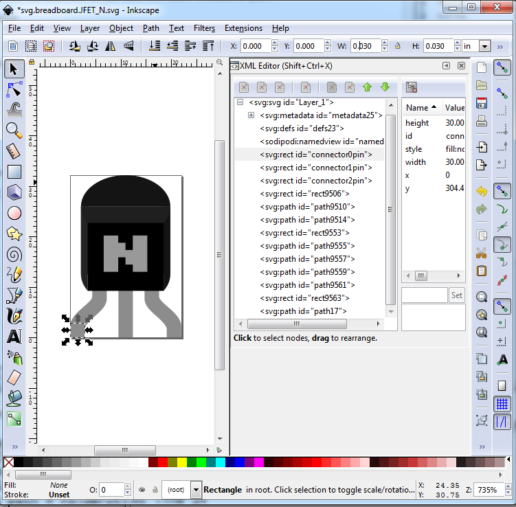
breadboard:
Currently a bendable leg part (although the fzp file isn’t configured that way)
so remove the 3 leg lines as unneeded.
ungroup
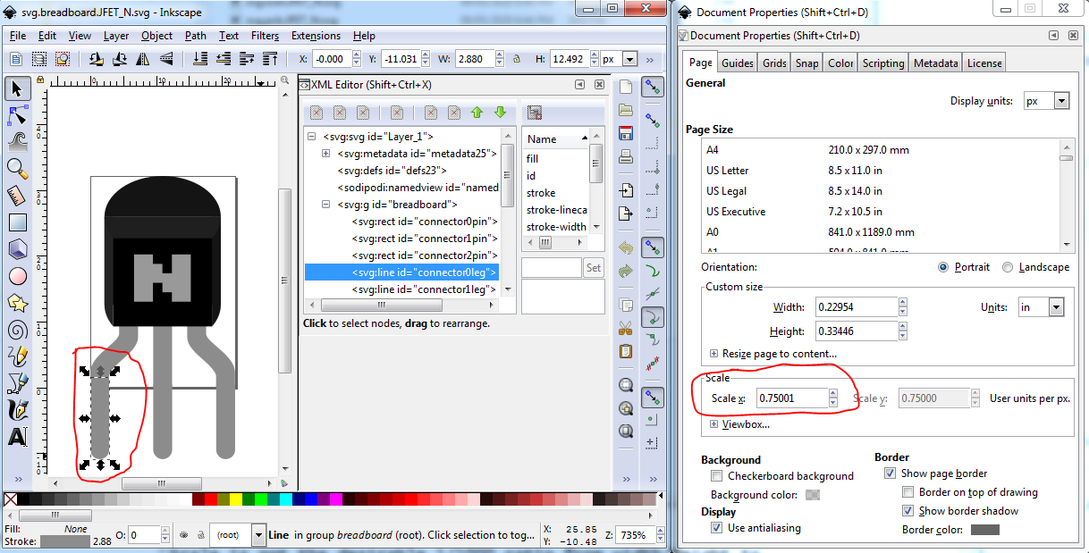
rescale explained here:
The pin is offset a bit in Y and not a square so correct that for a better pin appearance
If you really want a bendable leg part (I don’t like them!) just add back the legId to breadboard and the .fzp file.
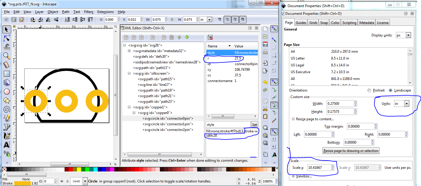
PCB
copper0 should be a child of copper1 and only one pin definition, (preferably pin on a through hole part. pad for SMD.) Silkscreen should be above the copper layers to make selection easier (the last group is first selected in pcb and you rarely want to select silkscreen!)
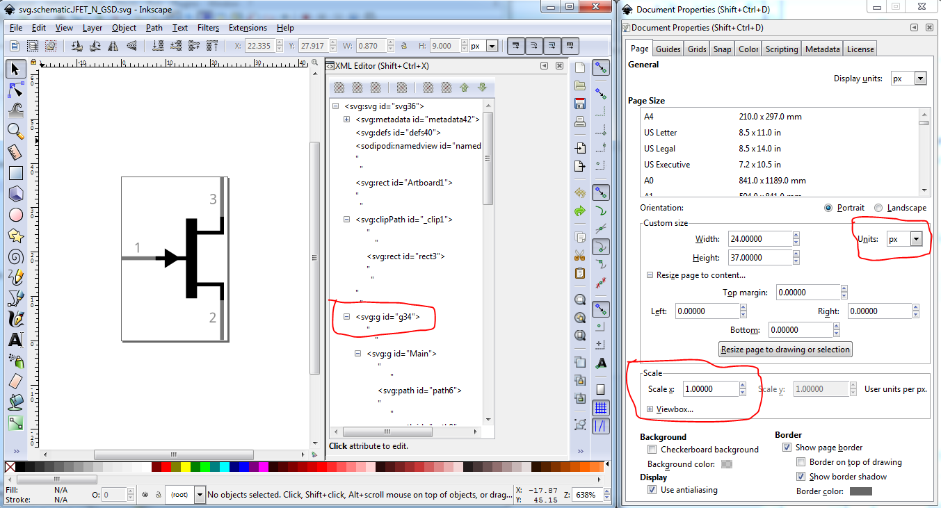
the g34 needs to be schematic to set the layerId. The only thing I know of that this affects is exporting the part as an svg (it won’t appear without the layerId.)
ungroup rescale
If the document is in px (rather than in or mm) Frizting will guess at which of the 3 DPIs was in use, 72DPI (Illustrator), 90DPI Inkscape < 0.9.2, or 96 DPI Inkscape > 0.9.1 and sometimes gets it wrong and misscales the part.
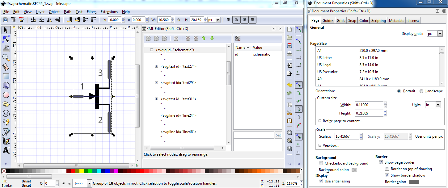
The scale of the image is slightly wrong (not enough to be the typical px problem I don’t think.)
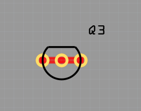
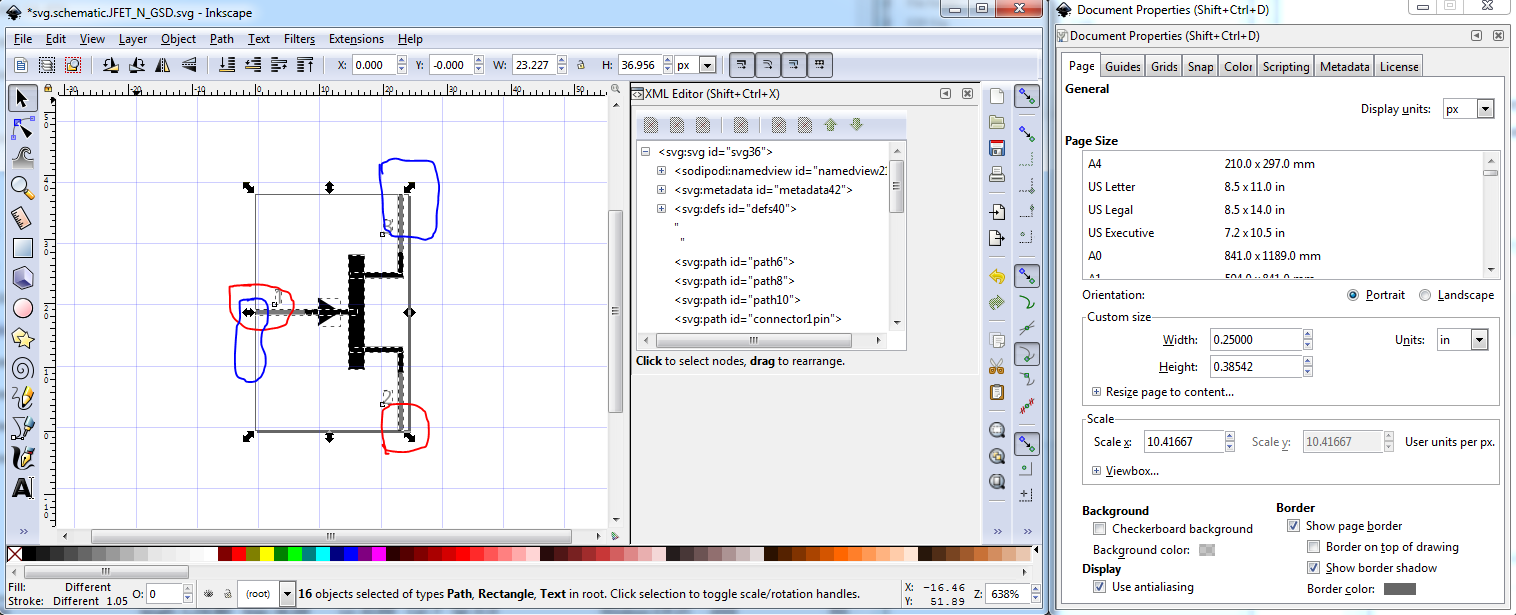
The pins should be on .1in boundaries to match other schematic parts. In addition the color of and width of the pins are incorrect, and the part is too big (space in schematic is at a premium so parts should be as small as possible.) With all that in mind I rescaled the part to use less space and match other parts better (and conform to the graphics standard for color)
Here pins are 10 thou wide, color #555555, with round line caps (at present different than the other transistors.) Lines in schematic are 10 thou wide so will match the pins. As well the part was compressed in to .1in * .2in to save space (and scaled appropriately to look right.) The terminalIds were converted to a 10thou * 10 thou invisible square and centered on the end of the pin. Corrected the pin numbering, the order was incorrect and did not match breadboard. Text font-family changed to ‘Droid Sans’, font size to 25px and fill to #555555.
fzp
correct Fritzing version, change moduleId change file names to convention
replace icon with breadboard svg (eliminates the icon svg file and saves space.)
remove terminalIds from breadboard defs (not used)
Change pad to pin in pcb view. All of which creates this new part (it will load along side your original as the moduleId has changed):