I am working on a PCB circuit layout where I want to isolate two parts of the PCB from each other using some sort of partition in the PCB layout. The circuit on one side of the partition will be powered with 5 volts DC. The other side will be powered by 12 volts DC.
Is there some way, using Fritzing PCB layout, that I can create the desired partition in the PCB’s copper cladding on both the PCB top and bottom?
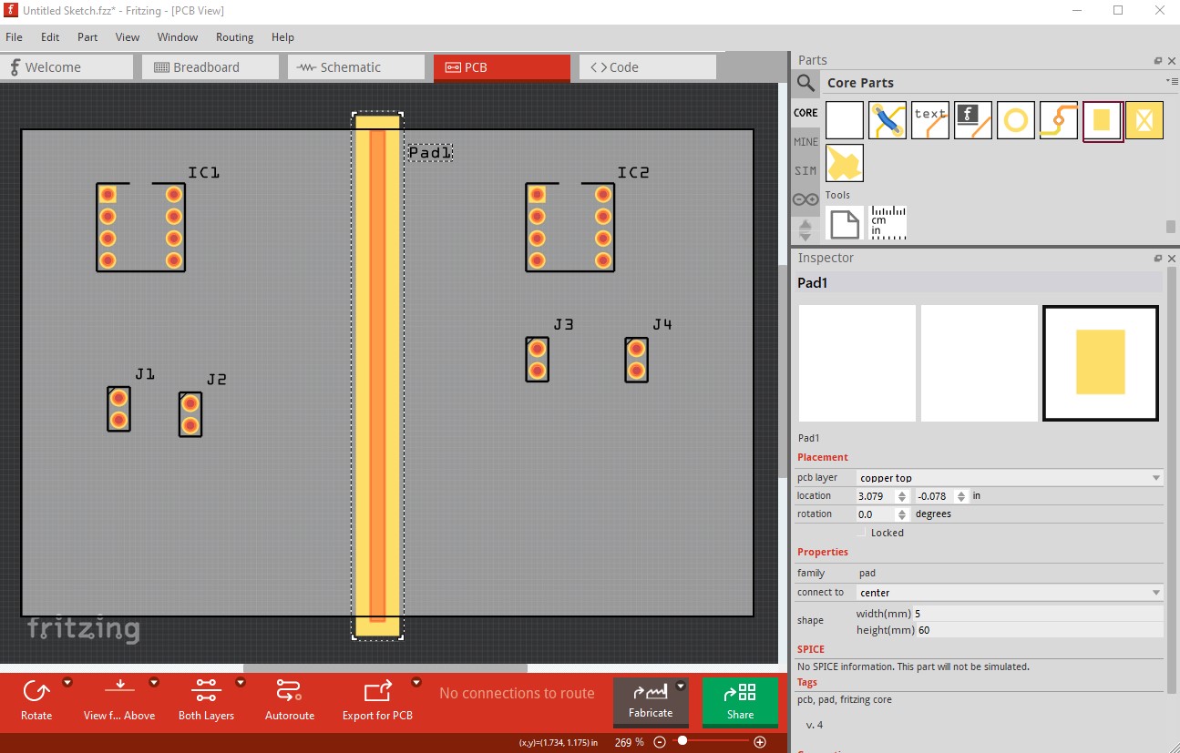
If I understand what you want correctly component placement should do what you want. Here I used a pad to mark the isolation area in the middle of the board. Place the 5V components on the left and the 12V components on the right then remove the pad to leave a blank isolation area.
Peter: Thank you! This operation is not obvious.
I did what you suggested and opened a new Fritzing board which is 60 mm high. I placed a pad, 65 mm high on this new PCB and added IC1 and IC2 as you did.
Then I removed the pad.
My PCB layout drawing shows no evidence of the pad being there, The is no indication that the copper on the top and bottom layers of the PCB shows no void between the left hand side of the PCB and right hand side of the PCB.
I expected to see a strip, 5mm wide, with no copper, where the pad had been. I did not see such a strip where the copper had been removed by this action.
No I don’t think so, removing the pad (which was just a visual marker of where the dividing line is) will leave a blank section of FR4 with no copper in it. An image of what you get and how that differs from what you want may help. If you don’t put any traces in the gap there will be no copper there unless you are doing a ground or copper fill. The case yo describe is what I would expect to happen.
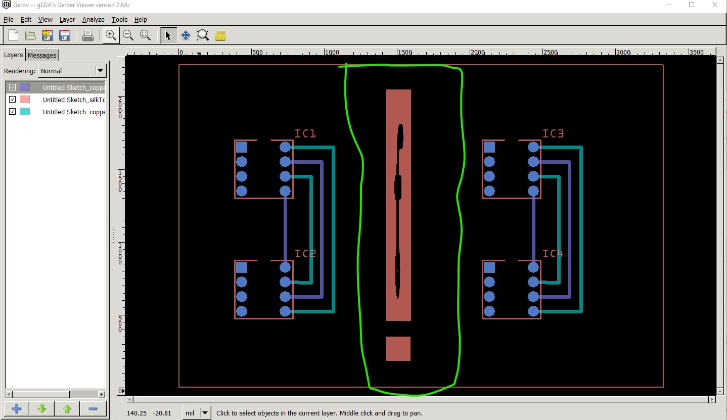
So this procedure gets the job done. It divides the two sections of the PCB. So if I do this procedure with the pad and send the Gerber for this board off to a board house, the fabricated PCB will come back with a gap in the copper where the pad was placed.
Is this what I should expect?
Also, does this procedure divide the PCB on the top and the bottom layer?
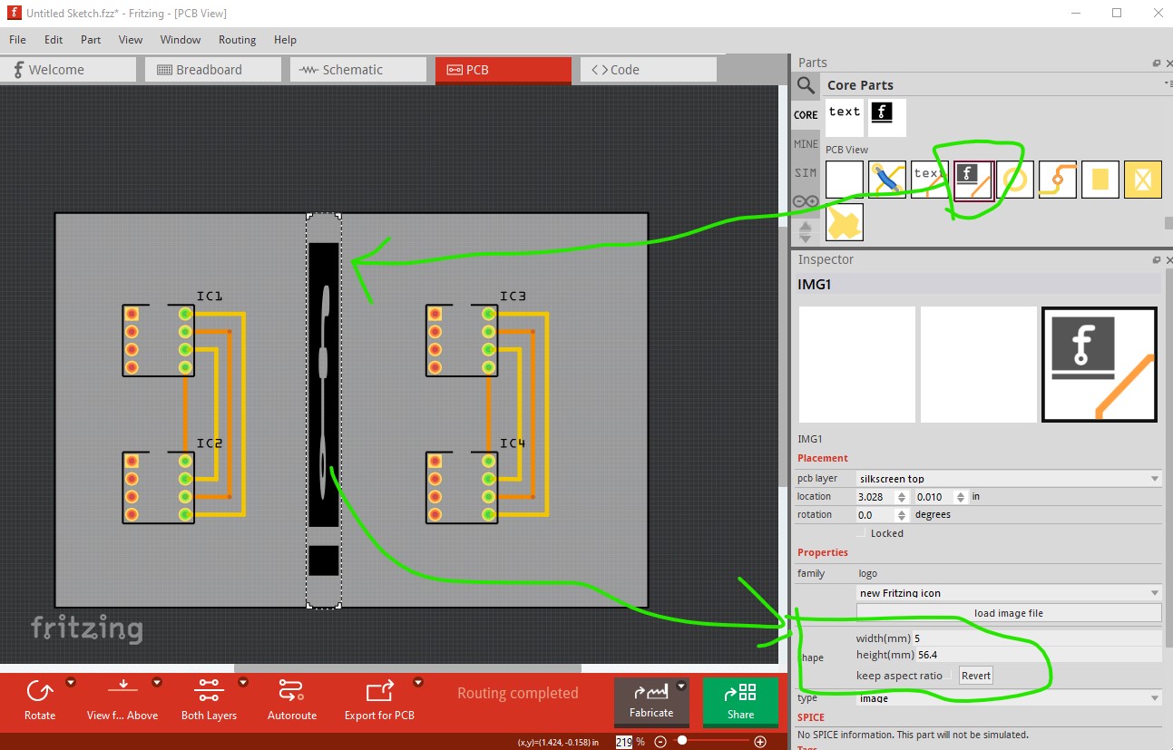
Yes as long as you do not run any traces in the keep out area. This sketch has two isolated circuits with an image file in silkscreen in the keepout area to mark it. I dragged in the image then unticked keep aspect ratio and set the height and width.
As you see there is no copper in the center area only the silksceen image. Solder mask will be covering that area but there is no copper (no green or blue lines) in it as long as you don’t run traces in it.
No the pad is only a visual marker so you know where not to run traces. The silkscreen image will do as well. The secret is not running traces where they shouldn’t be, Fritzing will happily let you run traces in the keepout area, to it copper is copper as long as it is inside the board boundaries. It will not enforce no copper there.