Good morning,
I want to create a small pcb (adaptor). I just need 16 pierced pads distributed over 4 rows and 4 columns with 8 connections between pierced pads.
I choose Stripboard1 with 4 rows and 4 columns and cut the 4 horizontal lines in the middle.
At this stage, I can’t make a PCB because it’s empty!
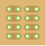
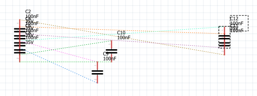
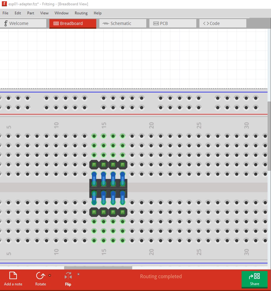
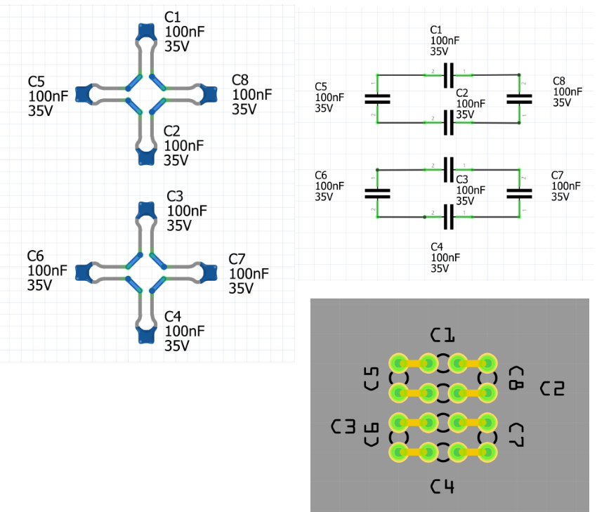
In the Breadboard tab, I add 8 ceramic capacitors which seem to me to be 1.27 mm pitch.
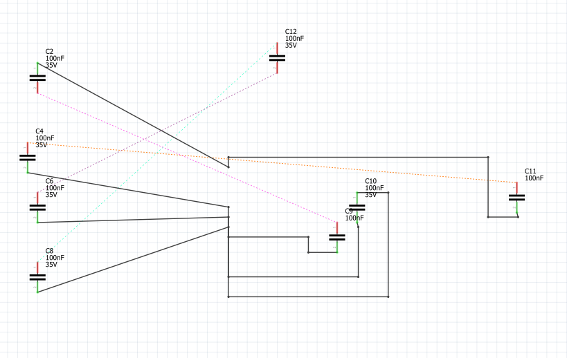
In the Schematic tab, I then obtain a diagram which means nothing and which respects neither the 1.27 mm pitch nor the orientation of the capacitors!
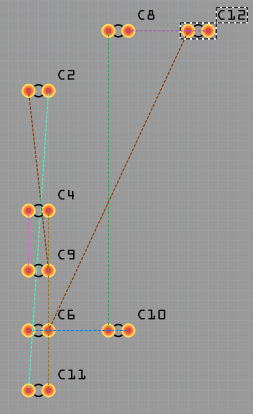
At this point, the single sided PCB is full of straps when none are needed.
I don’t understand.
Do you have a solution to make this super simple PCB?
THANKS.
This is normal. Strip board is intended to be strip board it does not create a pcb it only appears in breadboard. If you want pcb view you would need to create a custom part. The capacitors in breadboard are on 0.1in boundaries not 1.27mm (0.05in) note they match the 0.1in grid lines. As well searching for “top view” in the forums will find parts custom crafted from perfboard without the 3d view present here although that still won’t help with pcb directly. The capacitors will appear in pcb view but the strip board will not. To make this work well you would need a custom part that implements the perfboard pads in pcb (which likely doesn’t exist yet although it can be made.) with female pins so it will connect to the capacitors. Your problems in schematic are likely alignment. The connections in breadboard reflect in to schematic and pcb as rats nest lines. You need to rotate the parts in schematic and pcb until the routing is sensible. I would manually route them by clicking on the rats nest lines at that point as autorouter doesn’t work particularly well (no autorouter works all that well …) This would have been easier to explain if you had uploaded the sketch (the .fzz file, upload is 7th icon from the left in the reply menu) so I had the sketch to work from but these are the basic issues. In schematic view if you select Routing->Select all traces then hit the delete key it will delete all the wires leaving only the rats nest lines. Then move/rotate the various parts til the rats nest lines connect in a reasonable order (sometimes difficult because the connection will take the shortest available route which can cause issues) to get the parts correctly aligned.
Ok for these restrictions.
So is it possible to create a PCB without starting with a breadboard?
On a PCB, it is common to have connections with power and data input/output wires. I cannot find “components” allowing this type of connection to be made with only one side (a pierced pad connected to a passive or active component).
Hello and thank you for your answer.
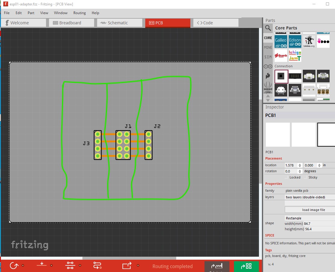
I placed capacitors to try to solve my problem of making a small PCB without components (in fact, I don’t need capacitors ). There will only be IC sockets cut in half. This involves making an adapter to place an esp8266-esp01 on a breadboard. Without an adapter this is not possible. The eight connections are in two columns of 4 rows with 2.54 mm (1/10th inch) spacing between connections.
On breadboards, to isolate the eight connections, the spacing (in the middle of the breadboard, where there are no holes) is 2x2.54 mm so you need an adapter.
Thank you for trying to resolve my issue but the solution is not suitable.
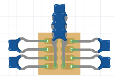
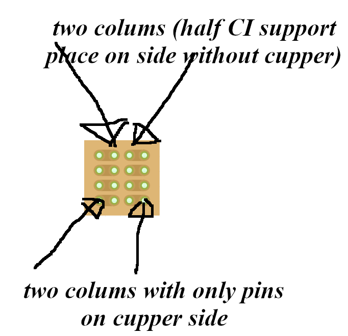
I cut an 8 pin integrated circuit support to have two columns of 4 female pins to plug in the esp8266 on the high side (without copper).
On the copper side, I solder two columns of 4 resistor legs to plug the adapter into a breadboard.
Of course, I can make this adapter by cutting a piece of prototyping board but I want to make my adapter using a Genmitsu 3020 pro max milling machine.
This is more difficult but it opens the door to much more complex achievements with the use of Fritzing.
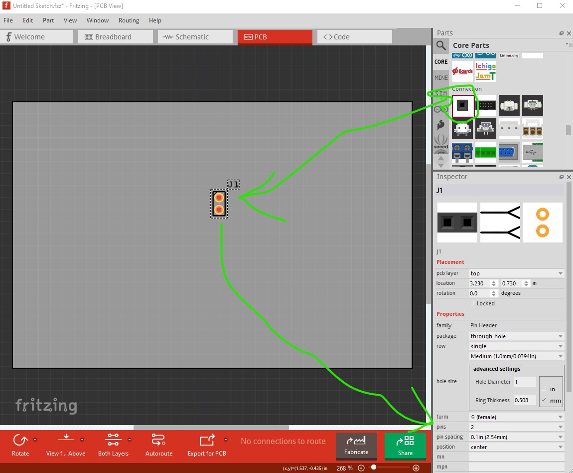
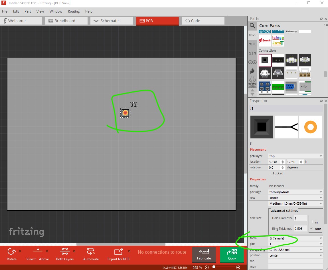
The two outside connectors are male, the middle dual row is female to accept the pins from the esp8266-esp01 which will then extend out over the breadboard which is not ideal as it blocks connections on one side or the other from the breadboard. A better solution would be an 8 pin IDE cable to connect to the esp8266-esp01 while allowing connections to the breadboard pins where the esp8266-esp01 would normally block them.
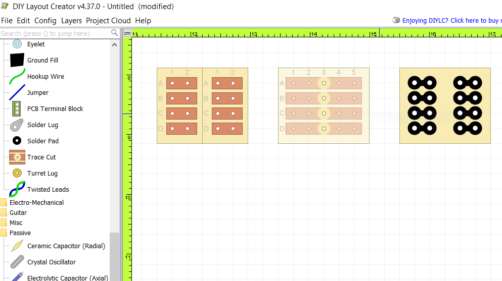
Perhaps this part will do what you want. I created it to match a physical implementation. Take a 2 by 10 header with long leads. Bend the leads on each side out, then back to get a .1 in offset. This was for an nrf24l01, but that has the same layout as the esp. It does not ‘look’ the same, but it should match the functionality of the board you want to mill.
Hello and thank you for your answers.
In the result I want to obtain, the distances between J1 and J3, on the one hand, and J1 and J2 on the other hand, are 1/10th of an inch. Exactly as in the first image in my post above (4 rows separated by 1/10th of an inch and 4 columns separated by 1/10th of an inch).
The microMerlin solution is interesting and perfectly meets the need for the adapter.
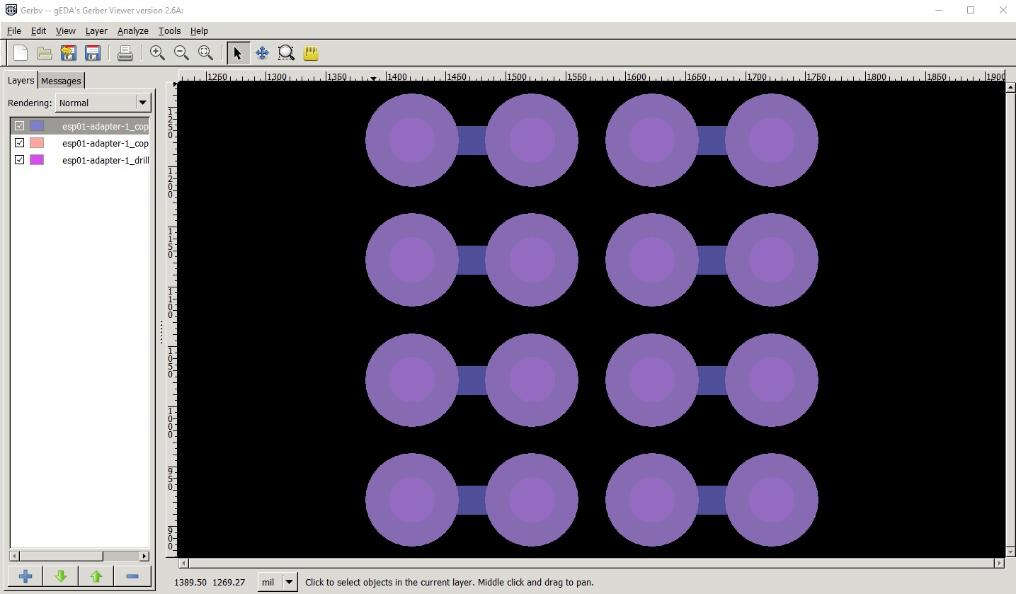
However, I am still listening for a solution to obtain a g-code in order to engrave a pcb with a cnc.
OK, that is a trivial change to the supplied .fzz like this. In turn the gerbers generated by that can be converted to g-code by the usual methods (there are instructions available in the forums search for g-code should find them.)
Yes. In the end up for what he actually wanted (which is a breadboard adapter for a wireless card with a dual row 0.1in header which wasn’t clear from the original post) a couple of headers in pcb does the job.
Good morning,
Based on the solution proposed by Claudius, I created the desired PCB. After going through FlatCam, the file generated is the expected one (verified with Candle).
Thank you all for your valuable help.
I’ll close this post (if I have the rights to do so ) adaptateur_esp8266_esp-01v3.fzz (4.3 KB)
While that certainly works the capacitors are essentially pointless and add clutter. The end result is identical to the .fzz I posted above (except there are no capacitors obscuring what you are doing.) A possible improvement would be to to make a custom part with a esp8266-esp01 like the one in this post
That is a lot more complex than just doing this in pcb, but it is possible. The easiest solution is to just use my original .fzz with the headers though (or your more complex if incorrect version with capacitors.)