Illustrator SVG Creation issue

Hello Fritzing:

When using Illustrator on Mac to create SVG I am getting a lot of errors when trying to “Load Image for View” within the part creator too.

I have tried so far 2 ways which both have their issues:

  1. Illustrator > File > Save As > Format SVG: Type (Tried SVG Profile SVG Basic 1.1, and SVG Tiny 1.2 as recommended:

This translates into the app crashing completely

Please don’t edit on these.
SVG Basic 1.1 exported code from Illustrator here
SVG Tiny 1.2 exported code from illustrator here

  1. Illustrator > File > Export > Export As > SVG (svg) using the following settings:

But when doing so it becomes like this on Fritzing:

instead of the file looking like this:

And here is the code of that outputted file (please don’t edit the file).

Please help, thank you.

Jules

I do not use Illustrator, but I can see that the generated svg is not valid for Fritzing. Fritzing uses the images like a CADD (drafting) drawing. It REQUIRES physical world dimensions to be able to properly size the part compared to other parts. Here is the svg header element from the SVG Tiny link you provided.

svg version="1.1" baseProfile="basic" id="Layer_1"
	 xmlns="http://www.w3.org/2000/svg" xmlns:xlink="http://www.w3.org/1999/xlink" x="0px" y="0px" viewBox="0 0 16 20.22"
	 xml:space="preserve"

It does not contain any width or height attribute, which need to be in real world units. Typically “in” or “mm” for inches and millimeters. Assuming that the 16 and 20.22 in the viewBox actually represent millimeters, adding width="16mm" height="22.22mm" should (I did not test how it looks) make it valid.

How to get Illustrator to add that you need to figure out.

1 Like

Thank you for your quick reply.

Sadly that did not work, added your suggestion:

<?xml version="1.0" encoding="utf-8"?>
<!-- Generator: Adobe Illustrator 25.2.3, SVG Export Plug-In . SVG Version: 6.00 Build 0)  -->
<svg version="1.2" baseProfile="tiny" id="Layer_1" xmlns="http://www.w3.org/2000/svg" xmlns:xlink="http://www.w3.org/1999/xlink"
	 x="0" y="0" width="16mm" height="20.221mm" viewBox="0 0 16 20.221" overflow="visible" xml:space="preserve">
<g id="silkscreen">

But it did not fix the issue I still get the following:

Overly Large copper sections and even the two black holes seem to have a copper outline despite not having any strokes.

Super strange.

[UPDATE] Adding Stroke value manually helped refine things up to this. Also the layer names were modified on the copper side.

The only last outstanding issue is the black holes which are now coperizzed… not sure why:

New code base here:

Thank you for the help

In addition to the height and width lack, there are a number of other problems here. Depending on what the associated .fzp file says, the copper0 name is likely wrong (and in the wrong order.) This is Inkscape rather than Illustrator but xml is xml.

should likely look like this:

assuming (as is usual) the .fzp file looks like this:

   <pcbView>
  <layers image="pcb/fc-51_85d98481ce3be6f2e9b641181c0f798b_1_pcb.svg">
    <layer layerId="silkscreen"/>
    <layer layerId="copper0"/>
    <layer layerId="copper1"/>
  </layers>
</pcbView>

The name and case of the layer identifiers in the svg need to match those in the.fzp file. Next, as it stands the pads won’t generate holes in the gerber output (although it will probably look fine in Fritzing) because the pads are paths (and not a circle which is the only path type gerber processing recognizes.) The pads need to look like this in xml

<circle
    stroke-width="20"
    stroke="#ffbf00"
    fill="none"
    id="connector0pin"
    gorn="0.2.0.1"
    cx="1173.0627"
    cy="177.96074"
    r="29"
  />

In Inkscape the hole diameter is hole = pad_diameter - (2 * stroke-width), I don’t know how Illustrator calculates them. The paths for slots won’t be processed at all (Fritzing has a hard time, as I’m told do most of the cheap board houses) with slots. The usual workaround is 3 over lapping holes to make the slot made by adding circles as above in addition to the path.

In Inlscape the diameter of the hole will be

hole_size - diameter_of_pad - (2 * Stroke-width)

I don’t know how Illustrator calculates this, as I believe it depends on how Illustrator calcultes the xml (it is different from Inkscape in Coral Draw for instance.) To upload svg files, you can zip the svg (it must be zipped otherwise the forum detects the svg and tries to render it) then rename the file to .fzp and tell us it is really a zipped svg. Upload is seventh icon from the left in the reply menu. There may be more problems here that I didn’t notice because FritzingCheckPart.py dies on the lack of height and width values (which I need to correct!) and is limited in its reporting due to the lack of the associated .fzp file. Usually uploading the complete .fzpz file for the part (which has the .fzp and all the svgs) is the best bet for getting help. Upload will accept a .fzpz file as well.

Peter

1 Like

I had a closer look at the SVG Tiny code. I think Peter may have looked at the other version. I see the outer layer, that is around “copper0”, is “copper1_1_”. That needs to match what is in the fzp file, but should probably be “copper1”. The black circles have copper rings because they are circle elements on the copper layer, and are getting the default stroke size (as you found for the connectors). Try adding an explicit stroke="none". I assume those are intended to be mounting holes. Often, the recommendation is put those on the silkscreen. There, gerber will not generate drill holes. If the user wants holes drilled, they drag one of the Frtizing “hole” elements over top the silkscreen marker. That way, the part can be used with or without the drill holes.

Also, check more than just what the part looks like in Fritzing. Do an export to gerber, and check the result with a gerber viewer. That will show things like the missing drill holes, because the connectors were defined as paths, without any circle element.

1 Like

Thank you both for the help, very very helpful!

So I added the mm and that helped with the scale.

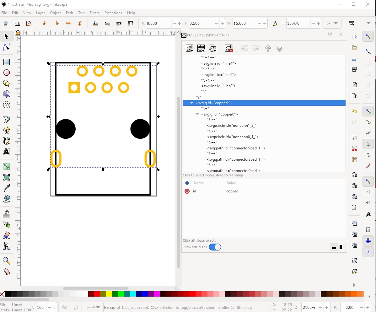
I also corrected the layering names to the proper ways.

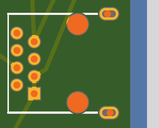
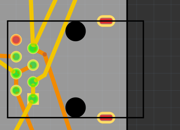
I also changed in illustrator the compound circles (one external circle, and one internal circle to determine the copper zone) and turned those into one circle with a stroke with a specific width which helped Fritzing recognize those and add a drill hole automatically in the center.

To fix the larger 2 drill holes I basically added another coper circle but with a very thin stroke which worked.

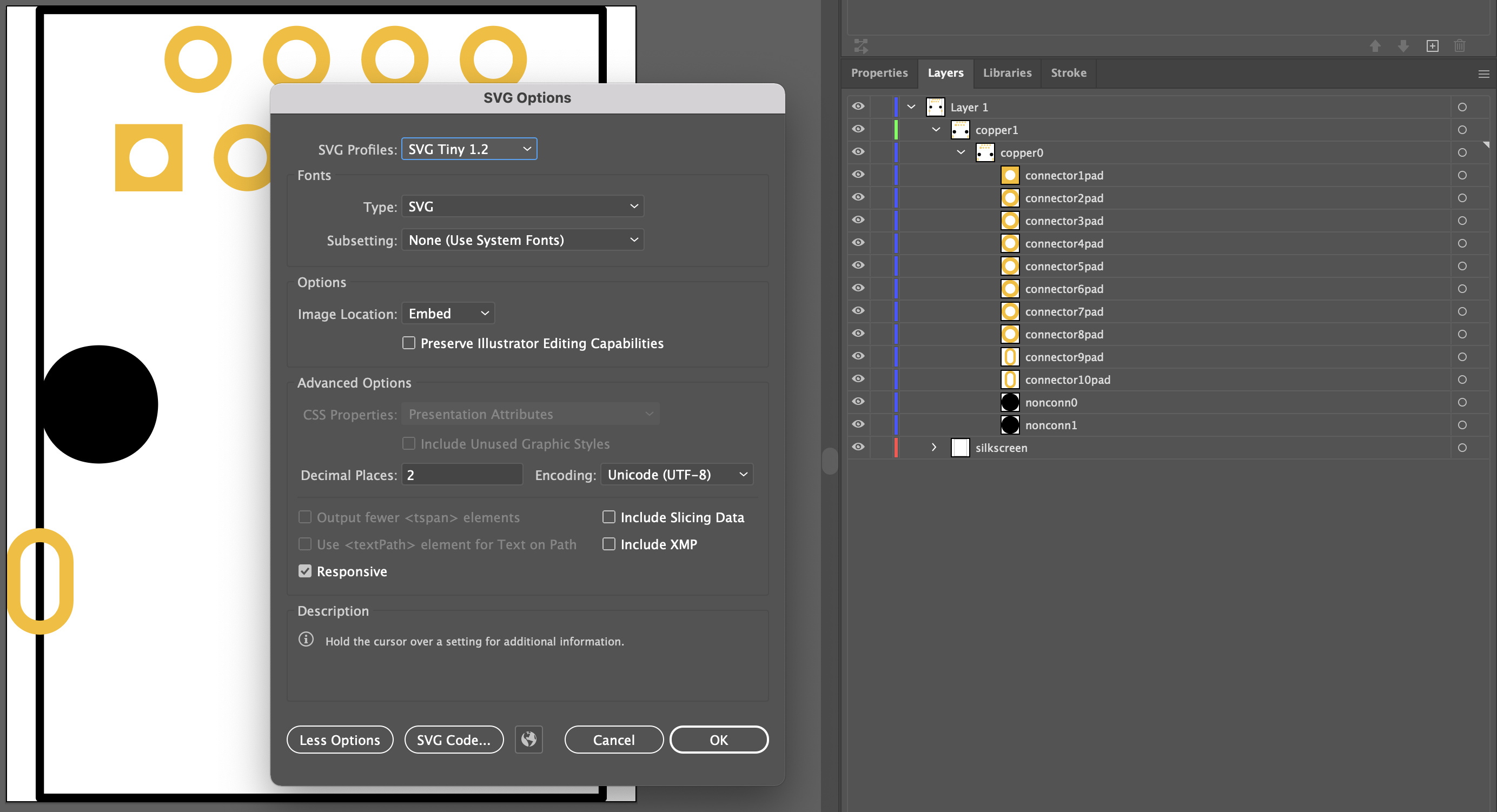
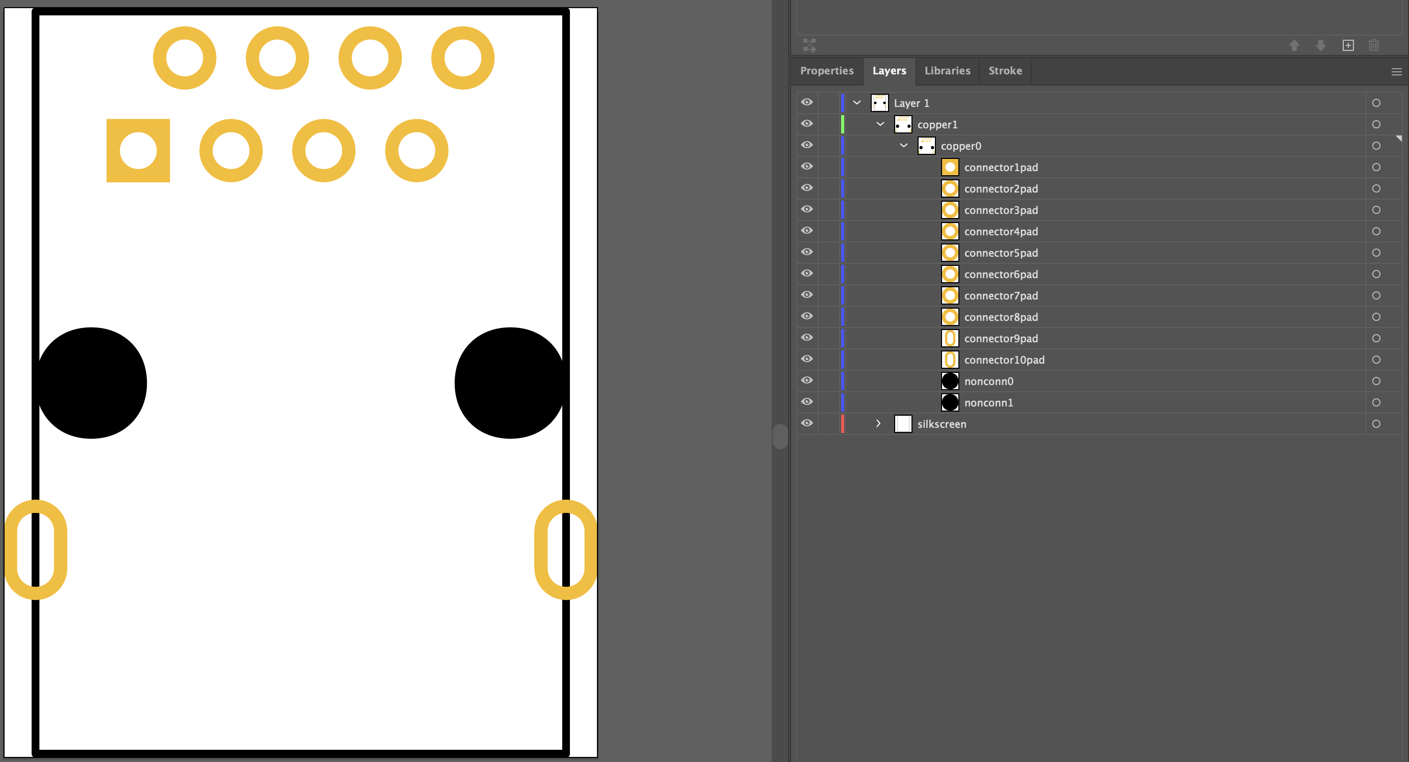
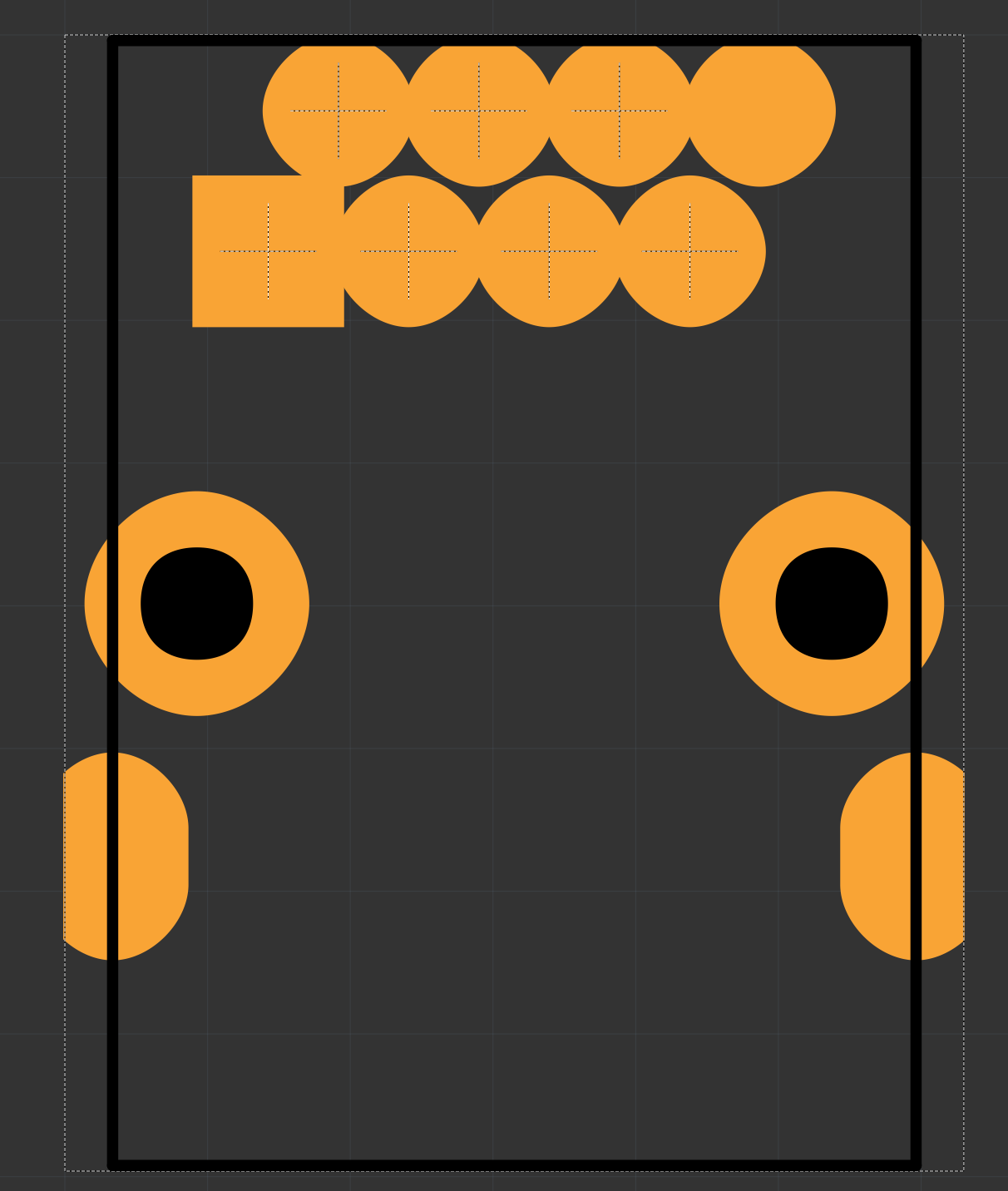
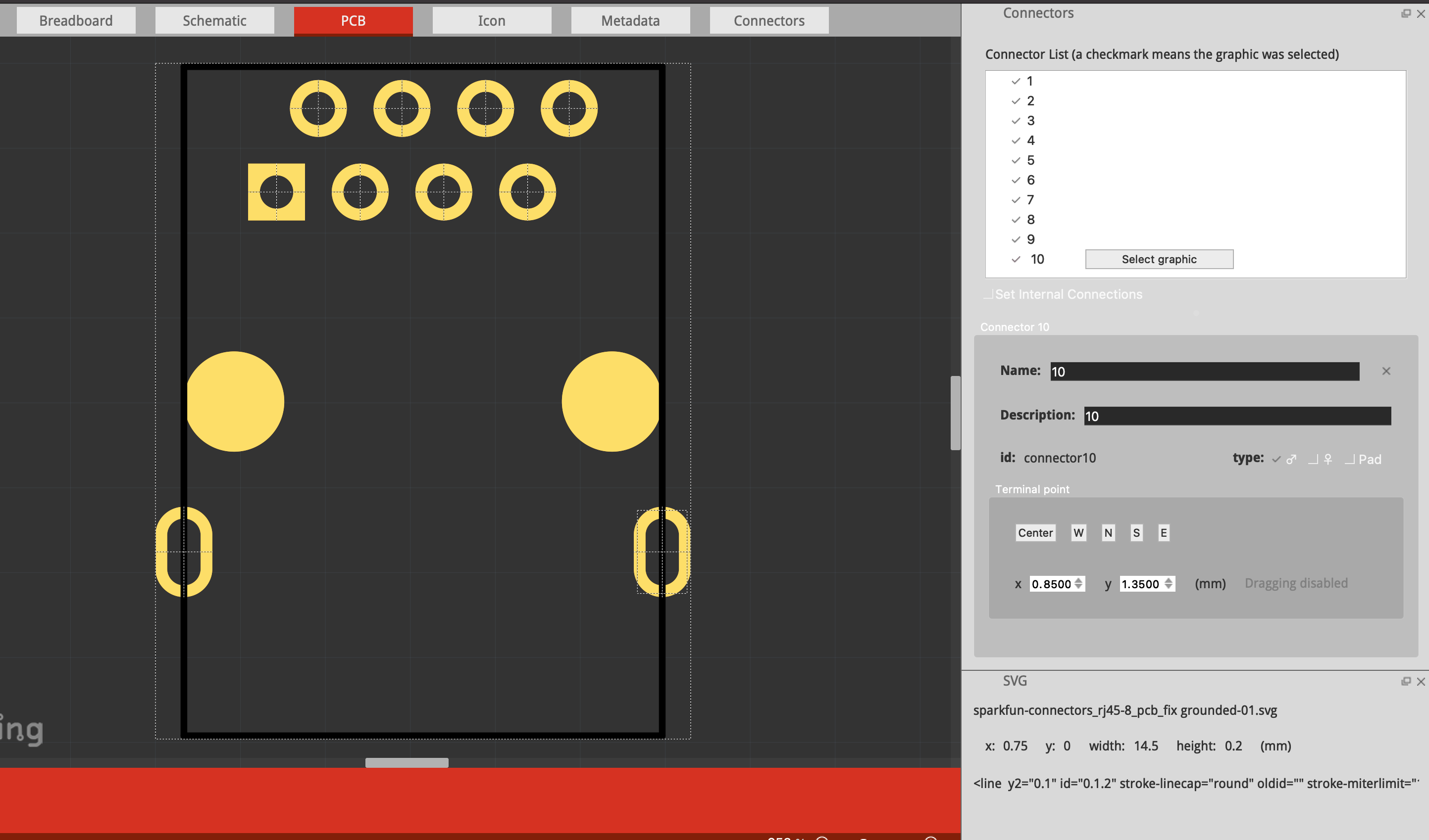
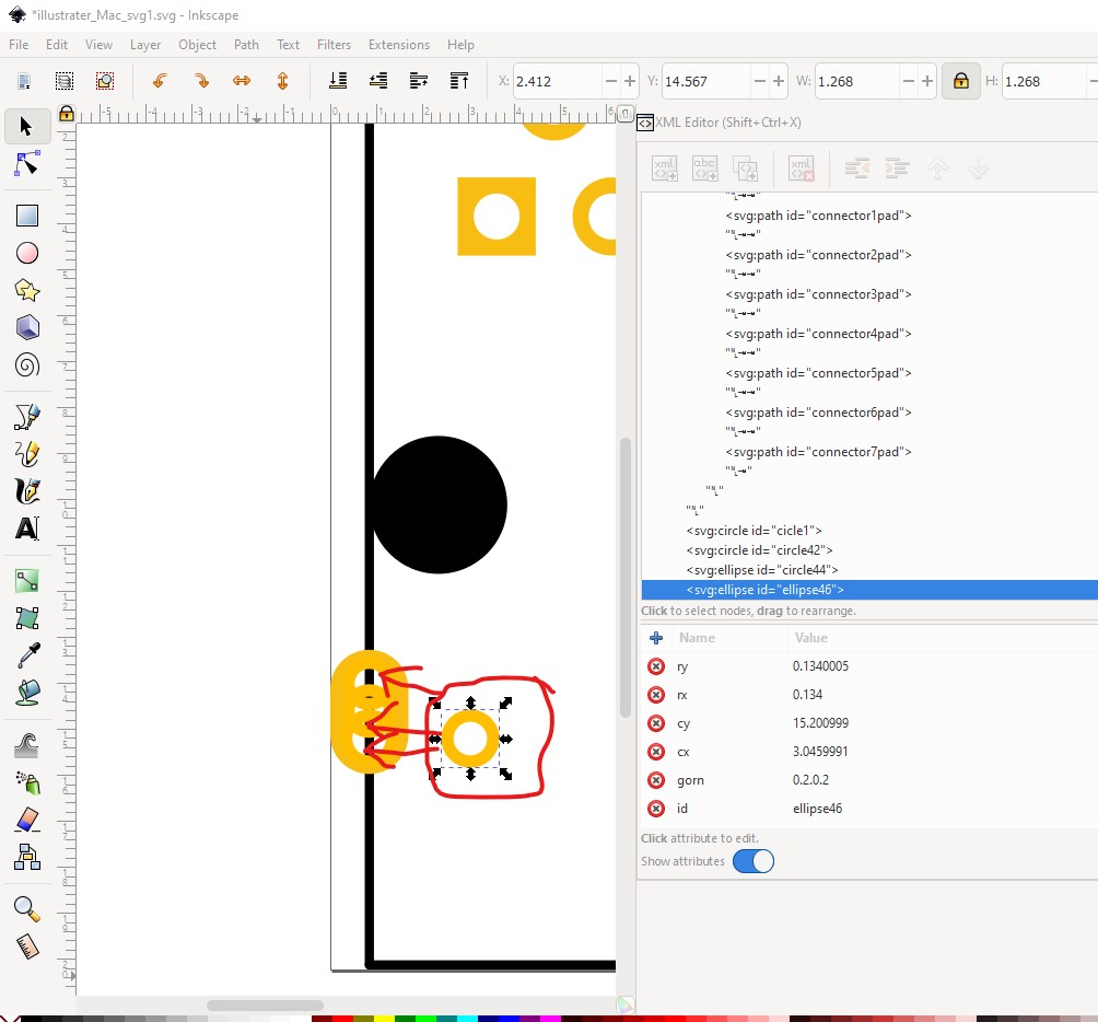
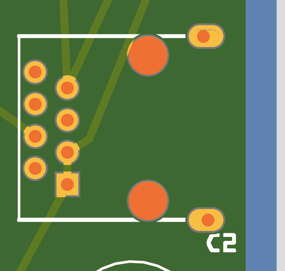
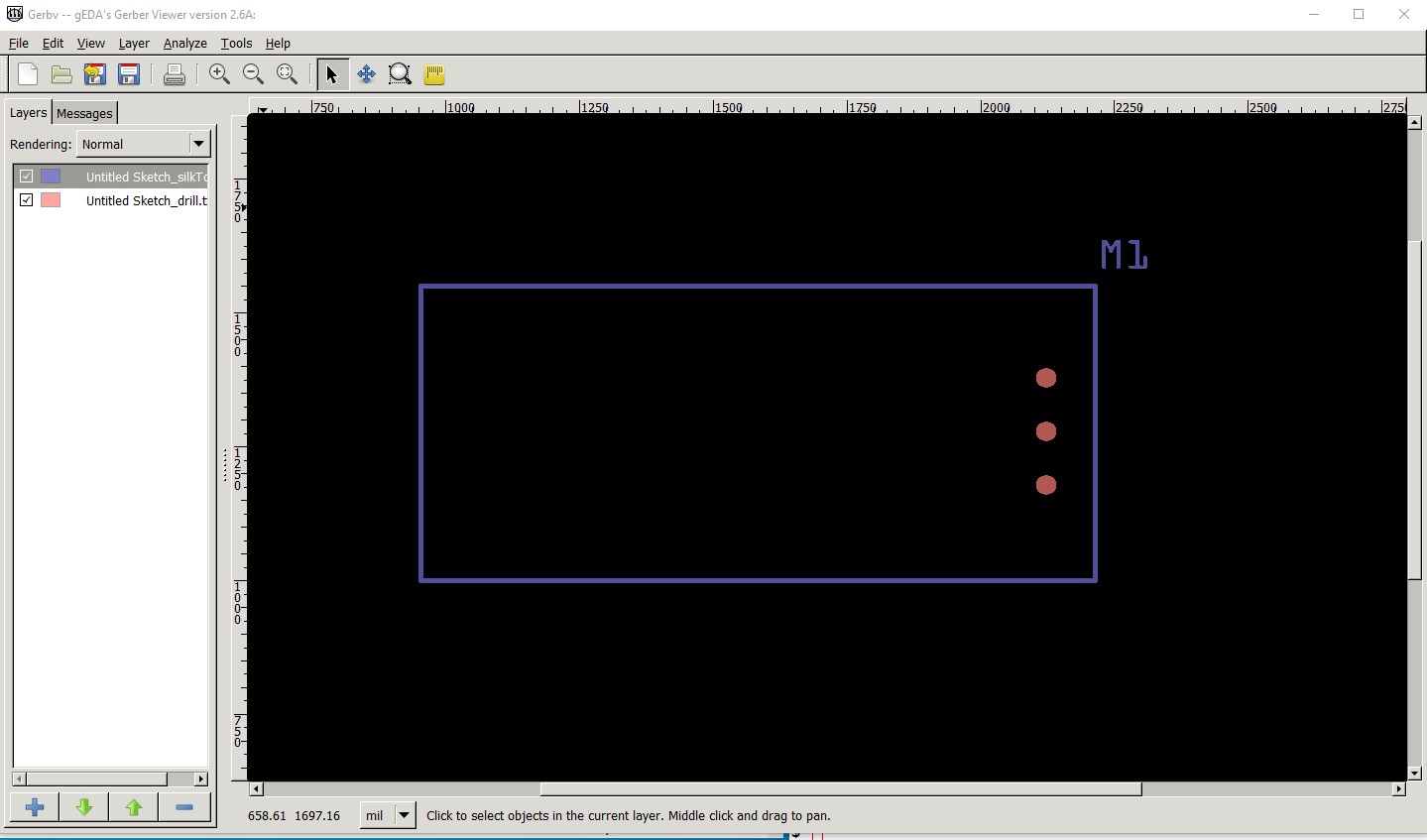
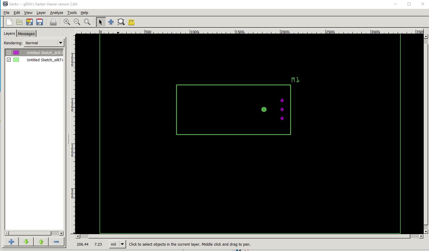
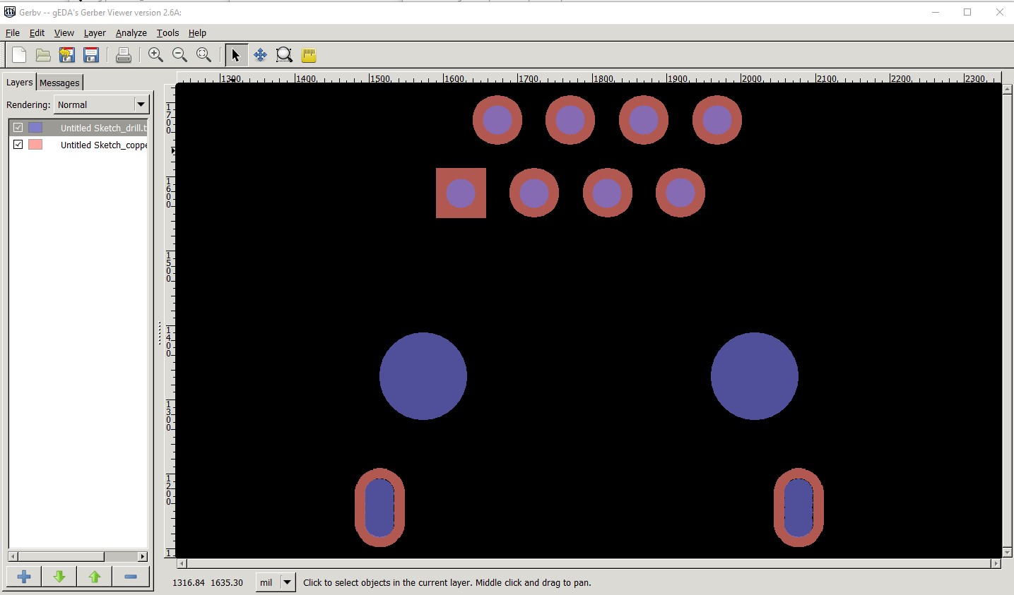
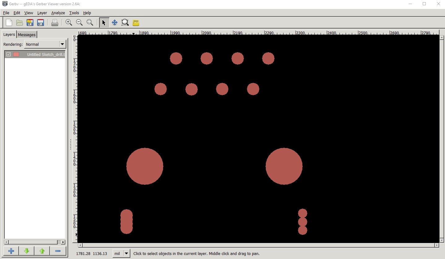
Now I still have a problem with the slot holes, those are not working with the 4 drill holes. Take a look at the file and how it comes out in Gerber format.

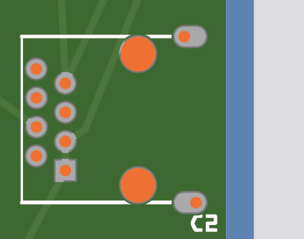
Which translates to (rotated 90º counter clockwise):

Screen Shot 2021-05-17 at 4.28.05 PM

And here is the SVG code so far:

<?xml version="1.0" encoding="iso-8859-1"?>
<!-- Generator: Adobe Illustrator 25.2.3, SVG Export Plug-In . SVG Version: 6.00 Build 0)  -->
<svg version="1.2" baseProfile="tiny" id="Layer_1" xmlns="http://www.w3.org/2000/svg" xmlns:xlink="http://www.w3.org/1999/xlink"
	 x="0" y="0" width="16mm" height="20.221mm" viewBox="0 0 16 20.221" overflow="visible" xml:space="preserve">
	<g id="silkscreen">

		<line fill="none" stroke="#000000" stroke-width="0.2" stroke-linecap="round" stroke-linejoin="round" stroke-miterlimit="10" x1="15.15" y1="20.121" x2="15.15" y2="0.1"/>

		<line fill="none" stroke="#000000" stroke-width="0.2" stroke-linecap="round" stroke-linejoin="round" stroke-miterlimit="10" x1="0.85" y1="0.1" x2="0.85" y2="20.121"/>

		<line fill="none" stroke="#000000" stroke-width="0.2" stroke-linecap="round" stroke-linejoin="round" stroke-miterlimit="10" x1="15.15" y1="0.1" x2="0.85" y2="0.1"/>

		<line fill="none" stroke="#000000" stroke-width="0.2" stroke-linecap="round" stroke-linejoin="round" stroke-miterlimit="10" x1="0.85" y1="20.121" x2="15.15" y2="20.121"/>
		<circle id="nonconn1" cx="13.65" cy="10.121" r="1.5" fill="#000000" stroke="none"/>
		<circle id="nonconn0" cx="2.35" cy="10.121" r="1.5" fill="#000000" stroke="none"/>
	</g>
	<g id="copper1">
		<g id="copper0">

			<circle id="nonconn1" fill="none" stroke="#F7BD13" stroke-width="0.01" stroke-miterlimit="10" cx="13.65" cy="10.121" r="1.5"/>

			<circle id="nonconn0" fill="none" stroke="#F7BD13" stroke-width="0.01" stroke-miterlimit="10" cx="2.35" cy="10.121" r="1.5"/>

			<circle id="connector10pad" fill="none" stroke="#F7BD13" stroke-width="0.35" stroke-miterlimit="10" cx="15.148" cy="14.12" r="0.673"/>

			<circle id="connector10pad" fill="none" stroke="#F7BD13" stroke-width="0.35" stroke-miterlimit="10" cx="15.148" cy="15.122" r="0.673"/>

			<circle id="connector10pad" fill="none" stroke="#F7BD13" stroke-width="0.35" stroke-miterlimit="10" cx="15.148" cy="14.488" r="0.673"/>

			<circle id="connector10pad" fill="none" stroke="#F7BD13" stroke-width="0.35" stroke-miterlimit="10" cx="15.148" cy="14.789" r="0.673"/>
			<path id="connector10pad" fill="none" stroke="#F7BD13" stroke-width="0.35" stroke-miterlimit="10" d="M0.174,15.121
			c0,0.373,0.302,0.676,0.676,0.676s0.676-0.302,0.676-0.676c0-0.001,0-1.001,0-1.001c0-0.373-0.302-0.675-0.676-0.675
			s-0.676,0.302-0.676,0.675C0.174,14.121,0.174,15.121,0.174,15.121z"/>

			<circle id="connector9pad" fill="none" stroke="#F7BD13" stroke-width="0.35" stroke-miterlimit="10" cx="0.849" cy="14.121" r="0.673"/>

			<circle id="connector9pad" fill="none" stroke="#F7BD13" stroke-width="0.35" stroke-miterlimit="10" cx="0.849" cy="15.123" r="0.673"/>

			<circle id="connector9pad" fill="none" stroke="#F7BD13" stroke-width="0.35" stroke-miterlimit="10" cx="0.849" cy="14.489" r="0.673"/>

			<circle id="connector9pad" fill="none" stroke="#F7BD13" stroke-width="0.35" stroke-miterlimit="10" cx="0.849" cy="14.79" r="0.673"/>
			<path id="connector9pad" fill="none" stroke="#F7BD13" stroke-width="0.35" stroke-miterlimit="10" d="M14.472,15.121
			c0,0.373,0.302,0.676,0.676,0.676c0.373,0,0.676-0.302,0.676-0.676c0-0.001,0-1.001,0-1.001c0-0.373-0.302-0.675-0.676-0.675
			c-0.373,0-0.676,0.302-0.676,0.675C14.472,14.121,14.472,15.121,14.472,15.121z"/>

			<circle id="connector8pad" fill="none" stroke="#F7BD13" stroke-width="0.35" stroke-miterlimit="10" cx="12.372" cy="1.349" r="0.673"/>

			<circle id="connector7pad" fill="none" stroke="#F7BD13" stroke-width="0.35" stroke-miterlimit="10" cx="11.126" cy="3.848" r="0.673"/>

			<circle id="connector6pad" fill="none" stroke="#F7BD13" stroke-width="0.35" stroke-miterlimit="10" cx="9.868" cy="1.354" r="0.673"/>

			<circle id="connector5pad" fill="none" stroke="#F7BD13" stroke-width="0.35" stroke-miterlimit="10" cx="8.625" cy="3.853" r="0.673"/>

			<circle id="connector4pad" fill="none" stroke="#F7BD13" stroke-width="0.35" stroke-miterlimit="10" cx="7.368" cy="1.353" r="0.673"/>

			<circle id="connector3pad" fill="none" stroke="#F7BD13" stroke-width="0.35" stroke-miterlimit="10" cx="6.122" cy="3.854" r="0.673"/>

			<circle id="connector2pad" fill="none" stroke="#F7BD13" stroke-width="0.35" stroke-miterlimit="10" cx="4.87" cy="1.351" r="0.673"/>
			<path id="connector1pad" fill="#F7BD13" stroke="none" d="M4.47,4.701h-1.7v-1.7h1.7V4.701z M3.62,3.35c-0.276,0-0.5,0.224-0.5,0.5
			s0.224,0.5,0.5,0.5s0.5-0.224,0.5-0.5S3.896,3.35,3.62,3.35z"/>

			<circle id="connector1pad" fill="none" stroke="#F7BD13" stroke-width="0.35" stroke-miterlimit="10" cx="3.623" cy="3.853" r="0.673"/>
		</g>
	</g>
</svg>

Ideally, there is another way to create cutouts in SVG other than a circle?

Let me know if you can think of anything.

Thank you!

Also tried this method with thinner copper stroke same issue:

The “nonconn” ids are not needed in silkscreen. The connector9pad connector10pad ids should only be on one of the circle elements. duplicate ids are technically invalid svg, though some things accept them. Fritzing will treat the content of the copper layers as copper, and join them to overlapping connectors without ids. Circles should generate drill holes whether they have an id or not.

You probably want one of the middle circles to be the one with the id. That is where Fritzing will draw traces to. Other things to try, to improve the look (without changing functionality):

  • make the path outline element the last in the set for a slot, and fill it with a color instead of none. That will visually draw over the rings from the overlapping circles.

  • You could also reduce the stroke width on the extra circles, and decrease their radius to match (reduce radius by 0.1 for every 0.2 decrease in stroke width). That will keep the holes, but make the ring smaller. The path element fills that in. Do not reduce the stroke to zero though. That would probably make them non-plated through.

Setting stroke="none" (or alternatively stroke-width="0") should work, instead of that thin stroke width for the mounting holes. Doesn’t gerber create a drill hole for that? The thin stroke might still cause the production house to try to create a plated through hole, from the way Fritzing will export to gerber.

Since these are through-hole, convention would have the names as “connector«n»pin” instead of pad. Pin works fine. As long as whatever is used matches the metadata in the fxp file.

Run design rules check on a sketch with the part and some traces. Those very thing traces on the overlapping holes might cause problems there. The rules Fritzing uses to match copper to associated connectors is based on the amount of overlap. The thin traces might not have enough overlap, and DRC would then complain that the part is on top of the copper, thinking that it is supposed to be separate.

1 Like

Worse than that, nonconn in silkscreen (as configured here in a test part) as I remembered appears in neither the drill file nor silkscreen (this is the drill and top silkscreen layers from gerbv with a noncomm1 circle in silkscreen)

There should be another hole to the left of the three pads as seen here. When the name in the pcb svg was changed to circle1 from noncomm1 it appears.

I’ll add an error for nonconn in silkscreen to FritzingCheckPart to catch this. It maybe should be reported as a bug as well.

Peter

1 Like

Which makes another reason to do the gerber export, and check the results for discrepencies. Not everything works the way you expect it too.

Thank you for your help.

So added your comments and the stroke-width=“0” helped for the large drill holes for sure.

It also helped to remove excessive coper for other drill holes.

So after cleaning up the ID duplicates and removing unnecessary ones and using Pin instead of Pad naming we get this now which is a step further in the right direction :slight_smile:

No more coper from Gerber but not all 4 holed in there for some weird reason.

Screen Shot 2021-05-18 at 3.29.45 PM

And yet in Fritzing we can see all four holes as such:

Screen Shot 2021-05-18 at 3.30.08 PM

So I wonder if there is a threshold to how close circles can overlap since I am using 4 in here instead of 3.

Or like one of you said naming?

Anyways here is the updated SVG:

<?xml version="1.0" encoding="iso-8859-1"?>
<!-- Generator: Adobe Illustrator 25.2.3, SVG Export Plug-In . SVG Version: 6.00 Build 0)  -->
<svg version="1.2" baseProfile="tiny" id="Layer_1" xmlns="http://www.w3.org/2000/svg" xmlns:xlink="http://www.w3.org/1999/xlink"
	 x="0" y="0" width="16mm" height="20.221mm" viewBox="0 0 16 20.221" overflow="visible" xml:space="preserve">
	<g id="silkscreen">
		<line fill="none" stroke="#000000" stroke-width="0.2" stroke-linecap="round" stroke-linejoin="round" stroke-miterlimit="10" x1="15.15" y1="20.121" x2="15.15" y2="0.1"/>

		<line fill="none" stroke="#000000" stroke-width="0.2" stroke-linecap="round" stroke-linejoin="round" stroke-miterlimit="10" x1="0.85" y1="0.1" x2="0.85" y2="20.121"/>

		<line fill="none" stroke="#000000" stroke-width="0.2" stroke-linecap="round" stroke-linejoin="round" stroke-miterlimit="10" x1="15.15" y1="0.1" x2="0.85" y2="0.1"/>

		<line fill="none" stroke="#000000" stroke-width="0.2" stroke-linecap="round" stroke-linejoin="round" stroke-miterlimit="10" x1="0.85" y1="20.121" x2="15.15" y2="20.121"/>
		<circle cx="13.65" cy="10.121" r="1.5" fill="#000" stroke="none"/>
		<circle cx="2.35" cy="10.121" r="1.5" fill="#000" stroke="none"/>
	</g>
	<g id="copper1">
		<g id="copper0">

			<circle id="nonconn0" fill="none" stroke-width="0" stroke-miterlimit="10" cx="2.35" cy="10.121" r="1.5"/>
			<circle id="nonconn1" fill="none" stroke-width="0" stroke-miterlimit="10" cx="13.65" cy="10.121" r="1.5"/>

			<circle id="nonconn2" fill="none" stroke-width="0" stroke-miterlimit="10" cx="15.143" cy="14.118" r="0.501"/>
			<circle id="nonconn3" fill="none" stroke-width="0" stroke-miterlimit="10" cx="15.143" cy="15.124" r="0.501"/>
			<circle id="nonconn4" fill="none" stroke-width="0" stroke-miterlimit="10" cx="15.143" cy="14.431" r="0.501"/>
			<circle id="nonconn5" fill="none" stroke-width="0" stroke-miterlimit="10" cx="15.143" cy="14.758" r="0.501"/>
			<path id="connector10pin" fill="none" stroke="#F7BD13" stroke-width="0.35" stroke-miterlimit="10" d="M0.174,15.121
				c0,0.373,0.302,0.676,0.676,0.676s0.676-0.302,0.676-0.676c0-0.001,0-1.001,0-1.001c0-0.373-0.302-0.675-0.676-0.675
				s-0.676,0.302-0.676,0.675C0.174,14.121,0.174,15.121,0.174,15.121z"/>

			<circle id="nonconn6" fill="none" stroke-width="0" stroke-miterlimit="10" cx="0.852" cy="14.122" r="0.503"/>
			<circle id="nonconn7" fill="none" stroke-width="0" stroke-miterlimit="10" cx="0.852" cy="15.127" r="0.503"/>
			<circle id="nonconn8" fill="none" stroke-width="0" stroke-miterlimit="10" cx="0.852" cy="14.454" r="0.503"/>
			<circle id="nonconn9" fill="none" stroke-width="0" stroke-miterlimit="10" cx="0.852" cy="14.79" r="0.503"/>

			<path id="connector9pin" fill="none" stroke="#F7BD13" stroke-width="0.35" stroke-miterlimit="10" d="M14.472,15.121
				c0,0.373,0.302,0.676,0.676,0.676c0.373,0,0.676-0.302,0.676-0.676c0-0.001,0-1.001,0-1.001c0-0.373-0.302-0.675-0.676-0.675
				c-0.373,0-0.676,0.302-0.676,0.675C14.472,14.121,14.472,15.121,14.472,15.121z"/>

			<circle id="connector8pin" fill="none" stroke="#F7BD13" stroke-width="0.35" stroke-miterlimit="10" cx="12.372" cy="1.349" r="0.673"/>

			<circle id="connector7pin" fill="none" stroke="#F7BD13" stroke-width="0.35" stroke-miterlimit="10" cx="11.126" cy="3.848" r="0.673"/>

			<circle id="connector6pin" fill="none" stroke="#F7BD13" stroke-width="0.35" stroke-miterlimit="10" cx="9.868" cy="1.354" r="0.673"/>

			<circle id="connector5pin" fill="none" stroke="#F7BD13" stroke-width="0.35" stroke-miterlimit="10" cx="8.625" cy="3.853" r="0.673"/>

			<circle id="connector4pin" fill="none" stroke="#F7BD13" stroke-width="0.35" stroke-miterlimit="10" cx="7.368" cy="1.353" r="0.673"/>

			<circle id="connector3pin" fill="none" stroke="#F7BD13" stroke-width="0.35" stroke-miterlimit="10" cx="6.122" cy="3.854" r="0.673"/>

			<circle id="connector2pin" fill="none" stroke="#F7BD13" stroke-width="0.35" stroke-miterlimit="10" cx="4.87" cy="1.351" r="0.673"/>
			<path id="connector1pad" fill="#F7BD13" stroke="none" d="M4.47,4.701h-1.7v-1.7h1.7V4.701z M3.62,3.35c-0.276,0-0.5,0.224-0.5,0.5
				s0.224,0.5,0.5,0.5s0.5-0.224,0.5-0.5S3.896,3.35,3.62,3.35z"/>

			<circle id="connector1pin" fill="none" stroke="#F7BD13" stroke-width="0.35" stroke-miterlimit="10" cx="3.623" cy="3.853" r="0.673"/>
		</g>
	</g>
</svg>

Thank you again from your help.

Also just tried the 3 circles instead of 4 same issue and tried putting the Copper slot before the holes same issue.

I don’t “know” this, but I think that the extra circles for the overlapping slot holes should NOT have the nonconn ids. They ARE part of connectors. One hole for the slot should have the connector?pin id, the others should not have any id. Or at least no id that Fritzing will treat as having a special meaning.

If you upload the generated part file, or better, the test sketch you are doing the export from, we can look for interactions between the the meta data in the fzp file and svg images. If we can generate our own gerber export, we can check that is not a difference in the environment being used.

Something I can see on the posted image, is that you have a trace overlapping a mounting hole circle. That will not work. running DRC should have reported that as a problem. That is not a problem with the part, but DRC could also report other things that are. It “might” complain about the nonconn circles overlapping the connection graphics.

The overlap with the mounting hole is one of the reasons that a “suggestion” is to put the mounting hole circles only on the silkscreen (often a cross hair instead of a filled circle). If the user of the part wants mounting holes to be drilled, they can place one of the standard core “hole” parts on the pcb, aligned with silkscreen markings. If the mounting holes are not needed, then it becomes valid to route traces across the silkscreen.

Here is a better version along with an explanation. The .fzpz file (which will load fine in to Fritzing) has a few extra pcb svgs with changes. The one ending in _pcb-nonconn.svg produces this gerber output:

which looks like exactly what you want, except that I doubt that it is producible as the drill holes are too close together. As well (because of the nonconn labels) the holes are not plated through. The svg ending in _pcb-correct.svg (which is also the current svg.pcb.fc-51_85d98481ce3be6f2e9b641181c0f798b_2_pcb.svg file produces this gerber output

the left slot is the same as the original. The right slot is what you need to use. The problem with the left slot is that there will be no board left for the drill to go through (the holes will likely be drilled in order) because the previous drill will have removed the fr4 already and the drill may snag and break. The one on the right is what people have told me they have used successfully. There is overlap (probably could be more overlap than here by a little bit) which leaves fr4 fir the drill tip to center on and cut. The edge isn’t as smooth but it doesn’t break drills. It would be a good bet to ask your board provider how close you can space ovelapping drill holes then adjust your circles to that. You will note that my 3 circles are labeled circle1 circle37 and circle39 (the latter 2 assigned by Inkscape when I duplicated the first one.) they don’t need connector numbers as they aren’t connectors just copper. This is also likely a case where the “put the mounting holes in silkscreen so the user has a choice of drilling them” doesn’t apply. This looks to be a connector of some kind that has tabs that are always on the part and thus always need to be drilled so the part will fit. The silkscreen advise if for modules that has flat mounting holes in the board but no tabs (and thus the user may not want mounting holes drilled.) Hope this helps.

Peter

Thank you both.

@ vanepp would you be able to provide me both version of these SVG’s? Would love to see how they are built out and how those translate on my end.

Thank you again.

If you unzip the test.fzpz file you will get the .fzp and all the .svg files like this which is an ls of the contents of the fzpz file. Fritzing doesn’t mind extra svg files in the zip as long as the ones it wants are there so I added the extra ones.

    part.fc-51_85d98481ce3be6f2e9b641181c0f798b_2.fzp
svg.breadboard.fc-51_85d98481ce3be6f2e9b641181c0f798b_2_breadboard.svg
svg.pcb.fc-51_85d98481ce3be6f2e9b641181c0f798b_2_pcb-correct.svg
svg.pcb.fc-51_85d98481ce3be6f2e9b641181c0f798b_2_pcb-nonconn.svg
svg.pcb.fc-51_85d98481ce3be6f2e9b641181c0f798b_2_pcb-orig.svg
svg.pcb.fc-51_85d98481ce3be6f2e9b641181c0f798b_2_pcb.svg
svg.schematic.fc-51_85d98481ce3be6f2e9b641181c0f798b_2_schematic.svg

What would be really desirable is to figure out if Illustrator will somehow let you set the scale or viewbox. I’ve looked at the Illustrator docs, but they seem to imply that mere users don’t need access to the internals but hopefully I haven’t known what to look for. This is the start of the breadboard svg in the above .fzpz, which is at the desired scale (in Inkscape 10.41667) which makes the viewbox 1000 * the document height/width in inches (so the internal units are 1000th of an inch)

    <?xml version='1.0' encoding='UTF-8' standalone='no'?>
    <svg
      xmlns:dc="http://purl.org/dc/elements/1.1/"
      xmlns:cc="http://creativecommons.org/ns#"
      xmlns:rdf="http://www.w3.org/1999/02/22-rdf-syntax-ns#"
      xmlns:svg="http://www.w3.org/2000/svg"
      xmlns="http://www.w3.org/2000/svg"
      xmlns:sodipodi="http://sodipodi.sourceforge.net/DTD/sodipodi-0.dtd"
      xmlns:inkscape="http://www.inkscape.org/namespaces/inkscape"
      id="svg2"
      y="0in"
      version="1.2"
      height="1.8474487in"
      width="0.55000001in"
      x="0in"
      viewBox="0 0 549.99998 1847.4486"

As noted, I 'm not sure there is a way but if there is it would great to know how to set it in Illustrator if that is possible.

Peter