I want to include a six pad ICSP programming connector on my arduino compatible board that I’m designing. I will then use something like this sparkfun Pogo Adapter to program the bootloader.
I just don’t really know what I should use on the pcb design for this, at the moment I have six copper pads arranged in the correct formation and sizing. Is this the done thing? However, the problem is when I view the design in a gerber viewer, these pads appear to have solder paste on them.
How do I ensure the copper pads do not have anything on the solder paste or solder mask layers?
Also, should these ICSP pads have some kind of drill holes like vias over them for the pogo pins to sit in? ( I’d prefer them not to because I’m pushed for routing space but if they are necessary I’ll put them in )
I’ll leave the solder mask question to one of the board gurus (I rarely make boards) although I don’t think there should be solder mask over pads as long as Fritzing thinks it is a connector, the pogo pins should work with or without the hole, but with a hole (and a pointed tip pogo pin as opposed to the multi contact head variety) there is somewhere for it to slide in to making alignment somewhat easier in a tight space (I assume you are using less than .1 inch spacing on the pads?). You also need to check that the pogo pins can be stacked together in the space you have (they work fine on .1 spacing and will probably do fine at least somewhat smaller) as I recall the sparkfun ones are fairly fine (I have a variety in different heads and from different sources, some of the cheap surplus ones I have are a lot larger than Sparkfun’s. Just some things to thing about
But for your connector, you are soldering to it and thus probably want flux. In fact for test/programming pads he also doesn’t want copper, but rather a gold connector overlay as for an edge connector on a PCB. I however have no idea how you specify that for a fab house, hopefully one of you experienced board makers can enlighten him (or perhaps he already knows). Copper on the pad will tarnish and likely not make contact with the pogo pin (which is also gold plated for that reason). This may not be something that Fritzing can do as well as I doubt it is very common in simple boards.
I think you can get away with high tin solder because it doesn’t tarnish that fast, or maybe not at all.
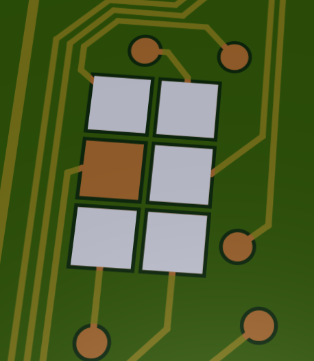
Like this
I have old circuits with high lead solder that is decades old and it has gone grey.
Yeah gold is the go.
I vaguely remember watching a fab video and you specify whether you want the gold added on top, but that applies to the whole PCB because it’s done by electro-plating, so that’s probably an extra. You can even get hard gold for sliding contacts.
Thanks. I have to keep the costs right down, I’m doing only two layers and the minimum board size for my purpose, I don’t think I can afford to use gold, is this a really expensive option?
At the end of the Sparkfun product video for the ISP pogo adapter I mentioned above, the guy demonstrates using the pogo pins on some boards, one is just onto bare vias and the other seems to be onto standard header pin holes. Is there a common practice for this?
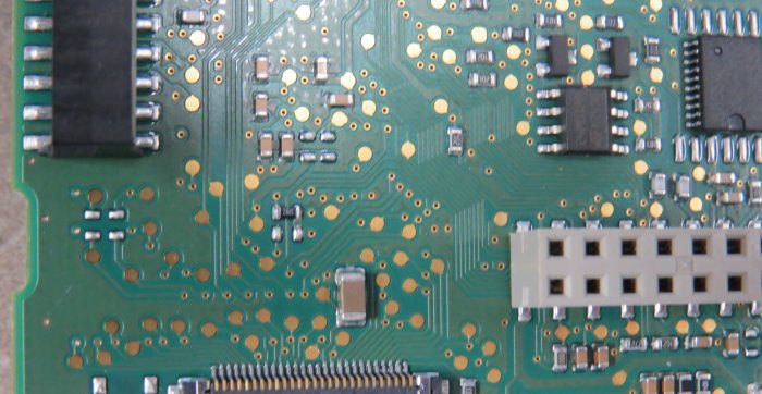
The issue I have with the solder paste appearing on the copper pads seems to be due to vias not being through the pad. Here is a screen shot of the ICSP pads on my board viewed in this gerber viewer. The only pad that does not have solder paste on it is the one I have put a via though. Please someone advise what’s going on. I’m new to all of this so please forgive my confusion.
I don’t know but I expect so as gold is expensive as is another step in making the board. As Old_Grey pointed out the pads are solder covered (rather than bare copper, my lack of board experience showing ) so that may work fine for you and will certainly be cheaper. I’d expect the pogo pins should make contact through the solder. It would be worth at least trying on a prototype board I expect.
I don’t think gold would be that expensive because it’s only microns thick.
I don’t know much about production houses either, because I DIY at home with a laser printer, a cloths iron, the safer ammonium persulphate, and a drill.
If you need use pogo pin.
this pogo pin catalogue for your REF.
2.54mm pitch connector Datasheet : https://www.pogopinconnector.com/Catalog/2.54mm-Pitch-connector-Catalogue.pdf
They have all kinds of Pogo pin Catalogue for your REF when you do design.
You don’t need to spend a lot of time looking for Pogo pin(Thread&Side Solder&Ball Point&DIP&SMD&Double Head&Right angle&Solder cup&Female Pin etc…) and USB Magnetic cable…Magnetic Connector… 1.27mm&2.0mm&2.54mm pitch pogo pin connector.

 ) so that may work fine for you and will certainly be cheaper. I’d expect the pogo pins should make contact through the solder. It would be worth at least trying on a prototype board I expect.