Found the problem. With “editable pin labels” set to true Fritzing substitutes a hard coded svg internally for schematic (presumably so it knows where the pin labels are.) I replaced my original part with one that has the schematic svg modified (and which looks invalid but isn’t as it will be substituted) to match the substitute svg so the labels and outline are in the correct place. Long term, I would like to remove that hard coded svg from the code because as noted it is ugly and violates the rule of least astonishment.
Yes the latest version that I replaced has the schematic svg modified (not completely, so it looks a little odd in Inkscape but works fine in Fritzing) to match what the code is substituting, so the part now appears correct in schematic in Fritzing. That only affected schematic, not the footprint. So long as you print out the footprint at 1:1 scale and check it against a real part to make sure it is correct, and verify the gerber output with a gerber viewer, your board should be fine. Feel free to upload your final .fzz file and I can check it over (not having the part I can’t verify the footprint though.)
I did check the footprint and it is an exact against the actual chip. However, I started to create a new pcb layout with the chip. and it seems to work ok until I ran the DRC (Design Rule Check) and I am getting all route to and from the chip reported as Overlaps. I tried a different chip from the library and I am getting the same result so it doesn’t appear to be a problem with PIC24FJ128GA204. I did try really thin wires but it still reports Overlay errors. Any idea why I would be getting these?
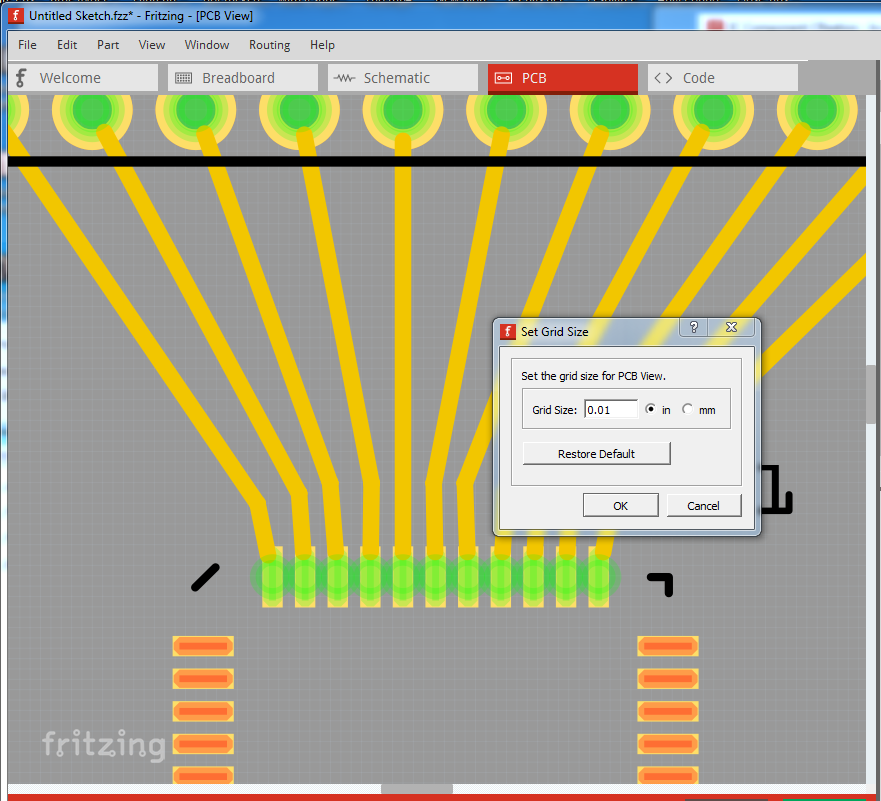
You need to set the grid size down to be able to position the traces far enough apart to pass drc. I’m using 0.01in (down from the default .1in) here and drc passes. You can also relax the default drc rules a bit for really fine pitch SMD but that shouldn’t be needed here.
I had to tweek the position of a couple of the right side traces a bit to get DRC to pass (if you click on the error in the DRC window it will show the conflict in red to tell you where to move.) If that doesn’t fix it, upload the .fzz file and I will have a look.
I reduced trace width to 21mm and relaxed the DRC rules - keepout is now .2140 mm. Do you think these are risky for fabrication? Anyway I have attached the FZZ file. Can you take a look at it and tell me which pins or spacing need to be adjusted?Untitled Sketch 2.fzz New.fzz (60.2 KB)
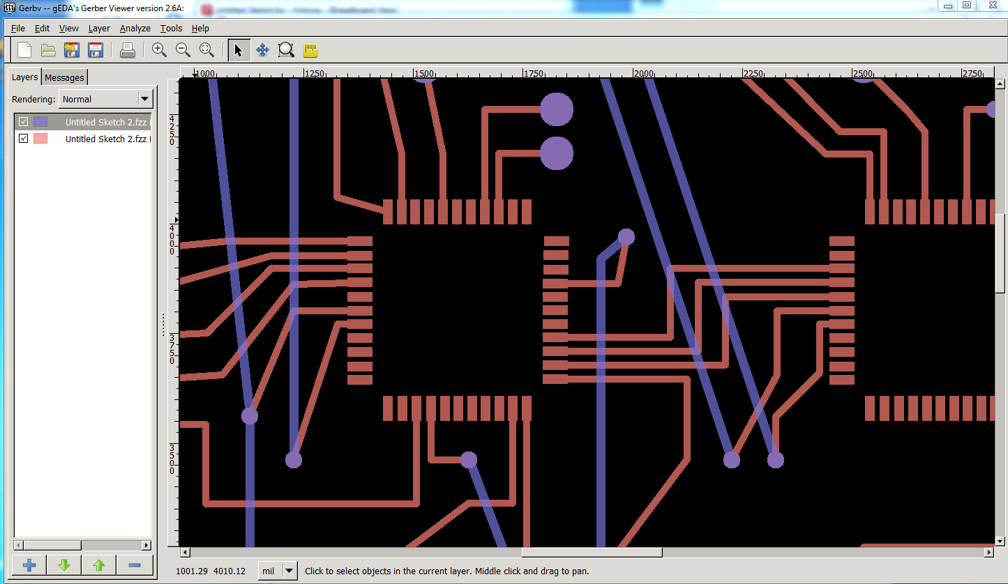
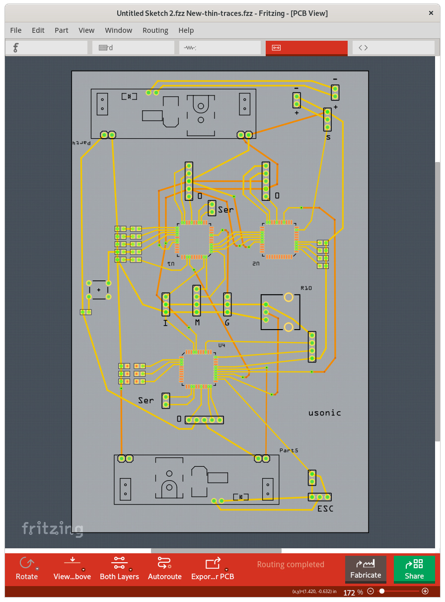
With the warning I’m not a big board expert (I rarely make boards) here are some suggestions: I’m not real sure why DRC is complaining (I may have screwed something up in the part but I can’t see it.) I did reduce the traces on the ICs to 16mils. If you click on a trace and look in Inspector (bottom right window) you can set the trace size to a variety of standard values. I have done parts with much finer spacing than this for people (one was running close to the 8 thou minimum clearance of the usual board houses but the chip worked fine and the user even managed to hand solder it!) One thing I would probably suggest is dragging schematic out and routing it to make sure the schematic matches what you thing you have routed in pcb (it is awfully easy to make mistakes!) The board house will make what the gerber says. I don’t think there will be any problem with this, as nothing but the IC traces (and not all of them) are tripping DRC and the gerber output looks fine to me ) this is the two copper layers gerber output in gerbv:
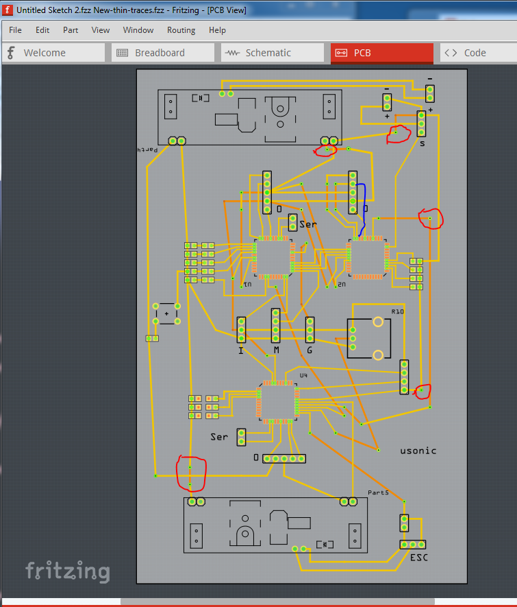
There are a couple of things (non critical) on the layout as well. There are a couple or redundant vias (circled in red here), in general less vias is better (one less chance of a plating through failure causing problems.) The one on the bottom via on the bottom left can be removed by selecting the bottom trace and clicking move to bottom layer (as the bottom most part is through hole.) Pcb best practice is considered all traces horizontal or vertical, with bends at 45 degrees and straight in to connectors (with a bend a bit out from the connector if required.) but this actually only matters at RF type frequencies and isn’t likely to be an issue here I don’t think. The blue wire on this image will eliminate one of the vias by routing the blue trace on the bottom layer to the pin on the header to a via on the blue wire by the IC (changing two vias in to one)
Peter
Thank you for the assistance - your comments are very helpful. Only Question -
Not sure what you mean by “One thing I would probably suggest is dragging schematic out and routing it to make sure the schematic matches what you thing you have routed in pcb”. Can you clarify?
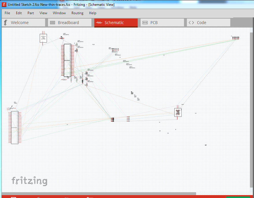
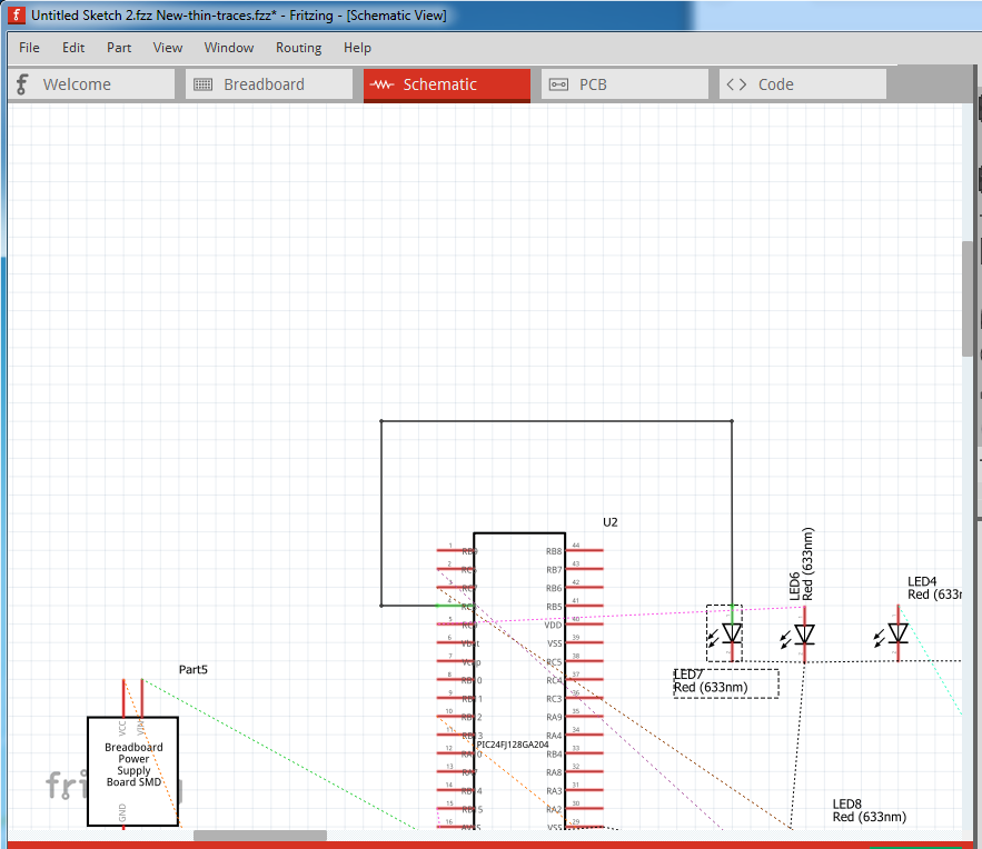
Many of the parts are currently on top of one another (a Fritzing quirk) so I clicked View->Ratsnest layer (which removes the ratsnest lines so they don’t select and form wires when you move parts), then dragged the components out to make this (where everything should be visible):
(rats nest is visible again to show connections though)
now you want to move things around to a sensible order to be able to route the schematic, and then select a rats nest line and double click on it to create the wire, them move the wire (just like a pcb trace) to route it sensibly:
Here I have done one of the LEDs (and not moved anything to a sensible position, not knowing what that is.) If you do this and only click on rats nest lines (it will let you make new connections that you don’t want quite easily and will reflect those changes as rats nest lines in to pcb!), then the schematic will match what was routed in pcb. If schematic matches what you think you routed all is well, but if there are mistakes they should show up as either missing , extra or mis wired connections in schematic where they should be easier to see than in pcb.
I did a bit of playing with this. Swapping a few traces between top and bottom layers, and minor route changes got rid of several more vias. Without repositioning any of the parts.
Moving parts around a bit could clean the routing up more, but I know nothing of the physical constraints you are working with for the headers and LEDs.
I ended up deleting a bunch of redundant bend points as well.