CD4518B Dual BCD Up-Counter
CD4520B Dual Binary Up-Counter
CD4520.fzpz (8.0 KB)
CD4518B Dual BCD Up-Counter
CD4520B Dual Binary Up-Counter
CD4520.fzpz (8.0 KB)
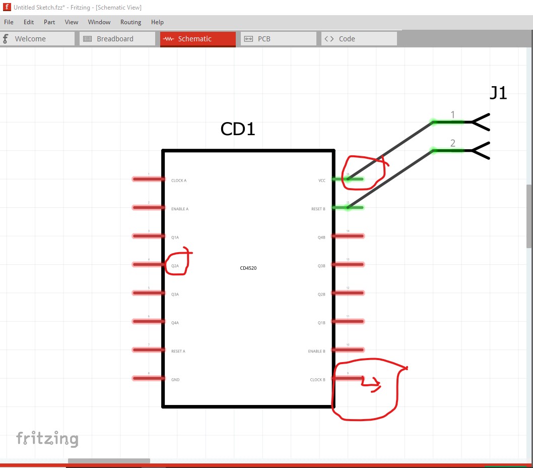
A number of problems here. Schematic lacks a layerId (and thus the part won’t export as an image), The terminalIds are present in the svg but not correct and are not present in the .fzp file so the wire connects in the center of the pin, the text font size is too small, and the part is offset about 0.05in in X and thus doesn’t align to the grid. As well the colors don’t comply with the graphics standard values. The easiest thing here would likely be to use the new Inkscape schematic extension described in this post:
to create a new schematic which will correct most of these problems.
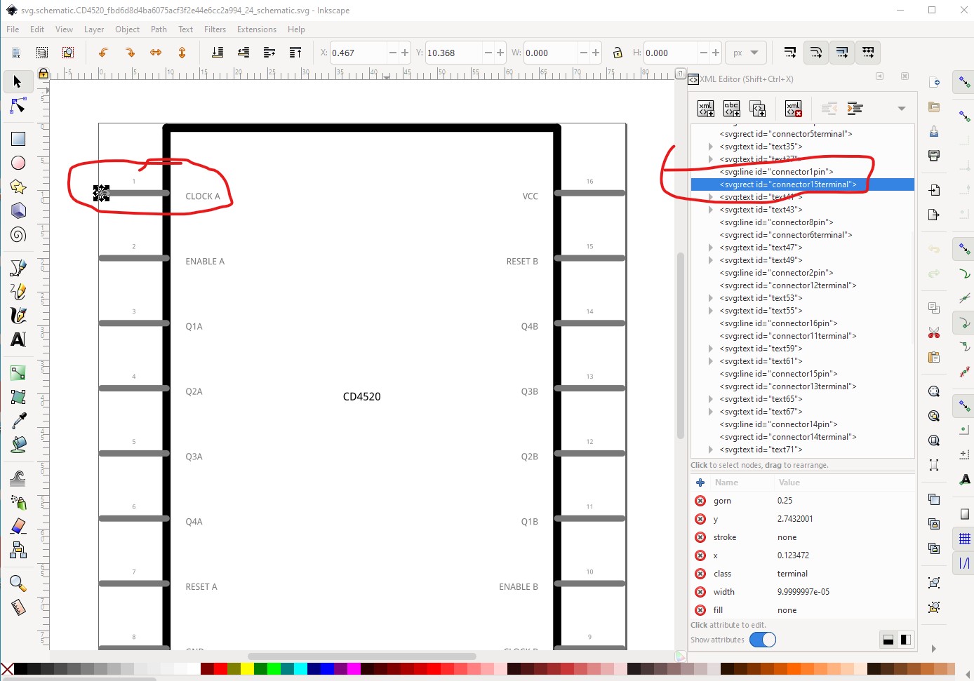
To fix the terminalIds you would need to edit the fzp file (or set the terminalIds in parts editor which will do the same thing) and add the terminalIds to the schematic view so:
   <connector id="connector1" name="CLOCK A" type="male">
      <description>CLOCK A</description>
      <views>
        <breadboardView>
          <p layer="breadboard" svgId="connector1pin"/>
        </breadboardView>
        <schematicView>
          <p layer="schematic" svgId="connector1pin"/>
        </schematicView>
        <pcbView>
          <p layer="copper1" svgId="connector1pin"/>
          <p layer="copper0" svgId="connector1pin"/>
        </pcbView>
      </views>
    </connector>
needs to change to:
   <connector id="connector1" name="CLOCK A" type="male">
      <description>CLOCK A</description>
      <views>
        <breadboardView>
          <p layer="breadboard" svgId="connector1pin"/>
        </breadboardView>
        <schematicView>
          <p layer="schematic" svgId="connector1pin" svg terminalId="connector1terminal"/>
        </schematicView>
        <pcbView>
          <p layer="copper1" svgId="connector1pin"/>
          <p layer="copper0" svgId="connector1pin"/>
        </pcbView>
      </views>
    </connector>
in the fzp file.
In this screen shot we see that connector1pin is associated with at terminalId of connector15terminal.
which doesn’t matter in this case because it is not defined in the fzp file.
PCB is by and large fine except the holes are 0.032in which is smaller than the standard 0.035in for IC pins and the connectors are named pad in the svg file:
but defined as pin (not pad) in the fzp file
        <pcbView>
          <p layer="copper1" svgId="connector1pin"/>
          <p layer="copper0" svgId="connector1pin"/>
        </pcbView>
but which Fritzing doesn’t appear to notice as the connections in pcb appear to work fine.
Peter
That offset is actually an illusion. It is caused because of the missing the terminalIds. The part alignment point is based on where the wires attach to the connectors. Since (without the terminalID) that is the middle of the connector, things appear to be offset by half of the length of the connector line.
Ah! Thank you! I looked at the svg and didn’t see anything that would explain the offset.
Peter
Lo estoy revisando pronto, gracias por las correcciones!!!