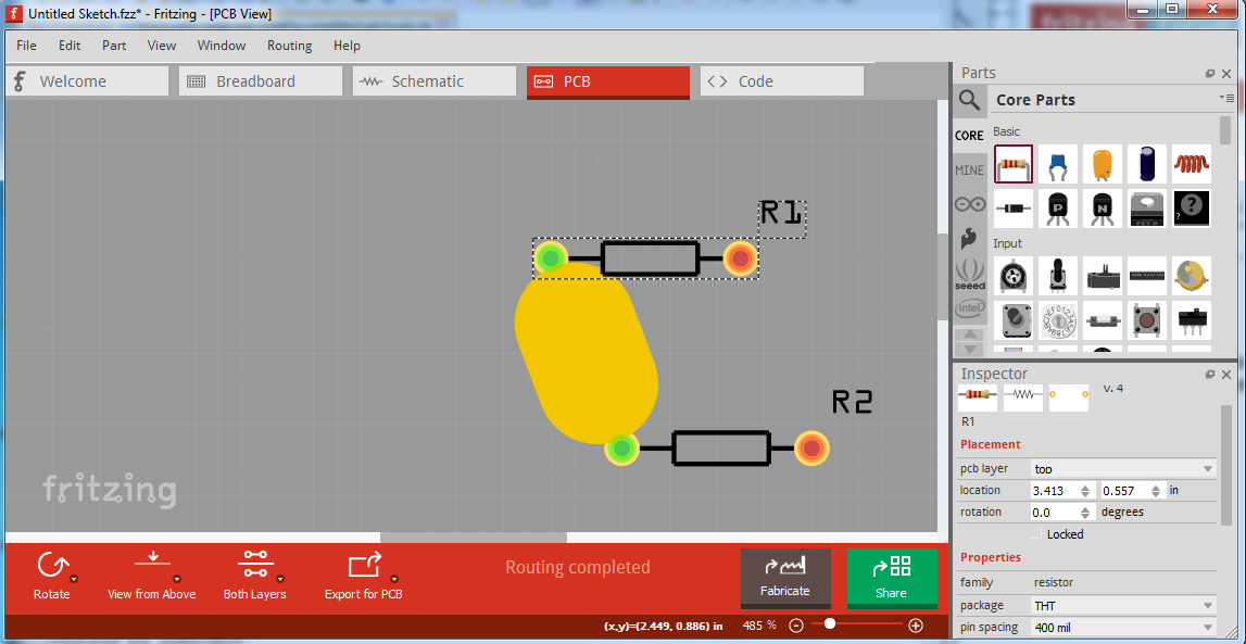
fritzing can provide 128 mil highest in pcb trace. And my local market provides 1oz copper pcb board. I need 30 amps to pass. For 1oz copper pcb how much trace should be used for my 30 amp connection??
Actually Fritzing will provide a maximum 255 mil trace if you type 255 in to the trace width field. The 128 mil width is only the p;ull down limitation. There is a bug in the gerber code that may make placing this exciting though (any largish trace, not just 255 mil.) the fix has not been commited yet, possibly due to a merge conflict that no one has so far had time to figure out.
Again google might be your friend. A search for “pcb trace width 1oz copper 30A” turns up
http://circuitcalculator.com/wordpress/2006/01/31/pcb-trace-width-calculator/
which claims to calculate trace widths given a variety of inputs. Never used this but it looks reasonable. You may well be better to look at one of the fabs that can do 2oz or more (if they do more) copper though for this kind of current as 2 oz copper halves the required trace width roughly which is a big win on board space. Also keep your high current traces as short as you can (i.e get it off the pcb in to wire as soon as you can.) Good luck!
Peter
1 Like
I used that calculator before this forum stuffs. But always shows me some weird values. That’s why I posted it in forum.
can’t type 255. It remains 25 (trace is just for example not specific for any device.)
And Thanks a lot for helping me out
By default it is in mils (1/1000 of an inch) thus the trace is large and it uses exponential notation:
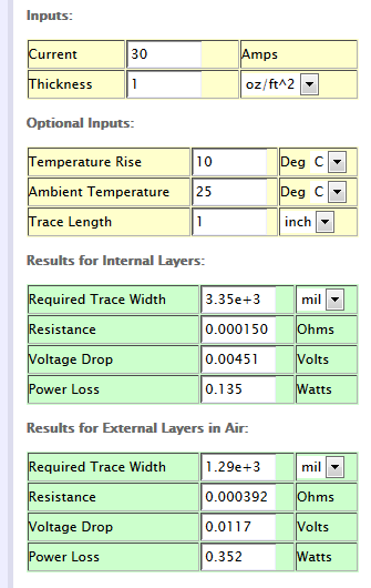
This is telling you for one oz copper and a 1in trace length on the top layer you need a trace width of around 1.3 inches or if you switch to mm
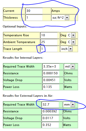
trace width of 33 mm which may be easier to read. Changing to 2oz copper cuts this in half. Lowering the length of the trace will also make it less.
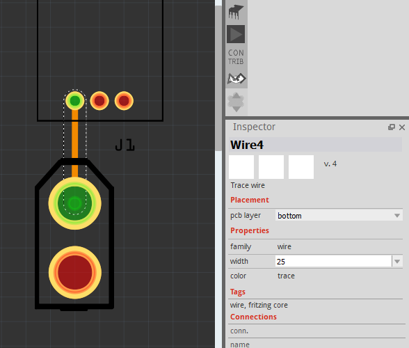
What Fritzing version? It looks like 0.9.3b (and this is 0.9.4 pre release, but 0.9.3b works the same) ?
Ah! You need to click on top (or another modifiable field) in inspector to make the change take (I do that without thinking about it and forgot to mention it the first time):
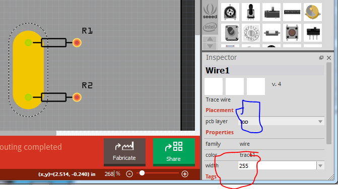
make the change circled in red then click on the blue circled icon to make the change take effect and you should be away. As a bonus this appears to work correctly in the gerber output (although that may mean the fix is in 0.9.4 and not in 0.9.3b so check your gerber output before ordering boards!)
You are most welcome. That is how I (and most everybody else) learned Fritzing, (because there isn’t a lot of documentation), by asking here. I’m paying forward lots of help from folks no longer posting here from years past. As well other folks will read this and learn how to do this.
edit:
For traces this large, you may well be better to use a copper fill. That said, I know very little about setting up copper fill, but some of the other folks here do.
Peter
1 Like
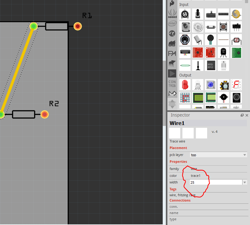
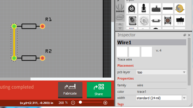
If you upload the .fzz file of your sketch, I’ll try it on 0.9.3b and see if I can figure out what is wrong. For me (as you see in the images) it accepted me typing 255 over the default 24. You may have to backspace over the 24 (so the field is blank) before you type the 255. It may feel it already has 3 characters for some reason.
edit:
I doubt this will work for you, I expect you will need to do a copper fill. It appeared to work correctly for me the first time because I did not move the resistors. Here I did with bad results. First, to enter the 255 in the trace width try selecting and backspacing over the selection so the select field is blank before trying to enter 255:
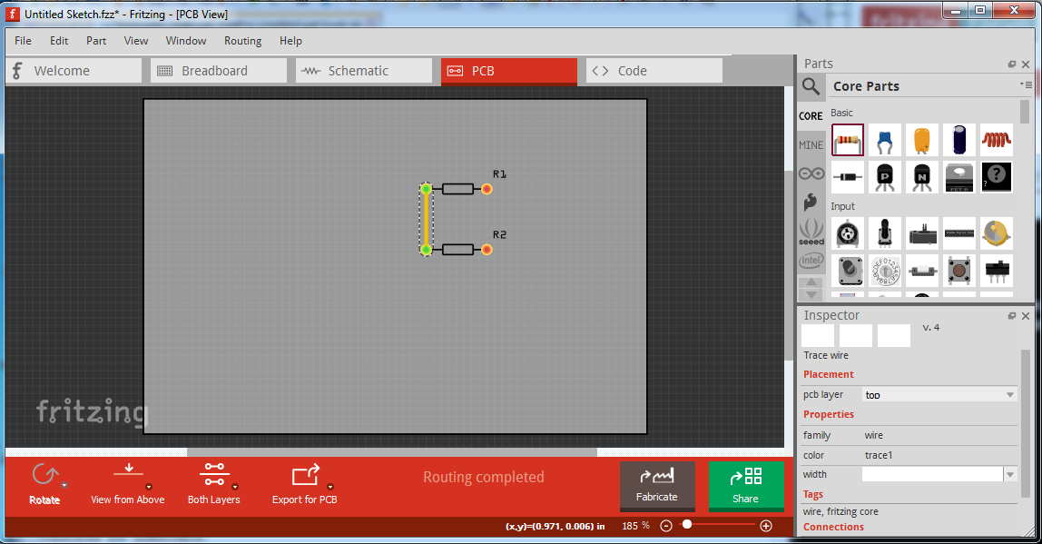
then type 255 in to the blank field and click on something other than the field and you should get:
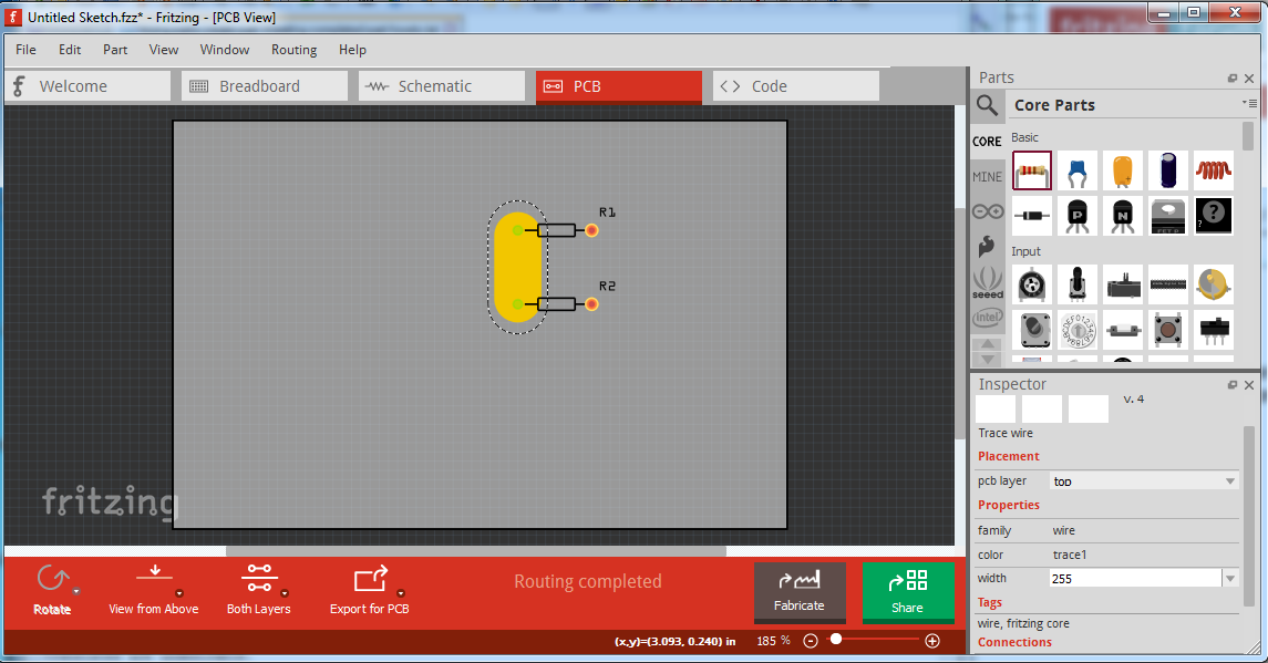
which looks correct, both in Fritzing and in the gerbers. However if you now move the bottom resistor right a bit, you get this:
Note the trace has moved from surrounding the holes (what you want) to being on the edge of the pads (not what you want for high current applications,) It looks the same in the gerber output:
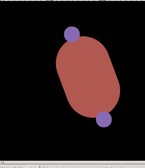
The blue pad will be a constriction point for the current and likely overheat. To do what you want I expect you will need to figure out how to do a ground fill to get the entire pad surrounded by copper.
Peter
sample.fzz (1.8 KB)
take my sample
Looks like my mistake. On 0.9.3b it is limited to 128 as a max value, on 0.9.4 pre release it allows 256. I suspect this is an unintentional improvement though, probably due to the new QT version in 0.9.4 because I don’t remember a commit for this. In either case I expect you will be better served by doing this as a ground fill to get maximum copper.
Peter
1 Like