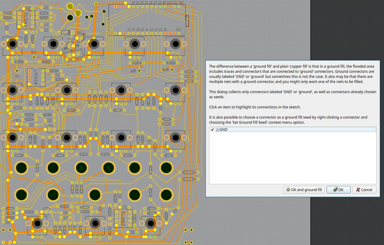
While working on a large PCB, I wanted to put a ground plane at the end. I’ve never done this before, but it seemed simple enough. However, when I set the ground seeds, selected “OK and fill”, nothing happened. I retried this multiple times, made a new file with a basic circuit with only a few resistors and had the same issue. Copper fills behave the same, whether from the routing menu or from the drag and drop copper fill part.
I also tried doing top layer, both layers, etc. Not just the bottom layer.
What I expected should have happened instead:
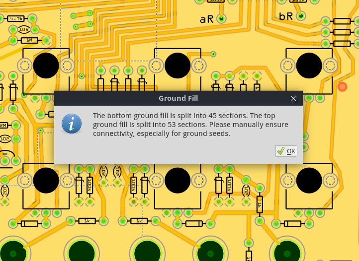
I expected there to be a visual indication that there was a ground plane - I double checked with a gerber viewer to confirm that the ground/copper fill did not in fact work multiple times.
My version of Fritzing and my operating system:
I am using version 1.0.5 on a standard version of arch linux.
Here’s me selecting the ground seed. An image wouldn’t really convey this, but the ground fill doesn’t do anything, nor the copper fill.
When I try to use the drag and drop copper fill from the parts menu, it says “Unable to create a copper fill–possibly the part was dropped onto another part or wire rather than the actual PCB.”
Two suggestions, if possible upload your sketch (the .fzz file, upload is 7th icon from the left in the reply menu) that would allow us to experiment (I have a copy of 1.0.4 and know how to access the old ground fill in it.) The second suggestion is to down grade to version 1.0.4 and try the old ground fill. There is a recently discovered bug in the new ground fill that isn’t (in that case, your mileage may vary ) in the old ground fill (which is no longer available in 1.0.5.) You can use the download link in your receipt from Fritzing.org to avoid having to donate again, older versions are available on the download page.. The original report on the bug it in the forum somewhere, the forum search bar should find it if you enter “ground fill” I expect. As I recall a fix was found by the developers but hasn’t yet come out (and may not make version 1.0.6 which is due soon.)
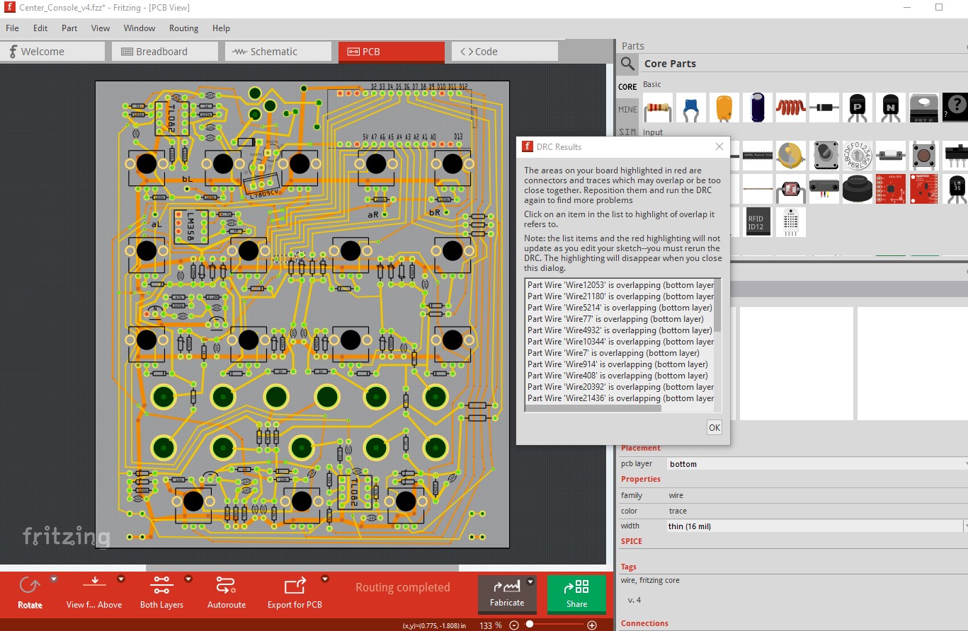
The other advantage of uploading the sketch, you get (hopefully helpful) criticism like this. Your board has DRC issues and is thus unlikely to work correctly.
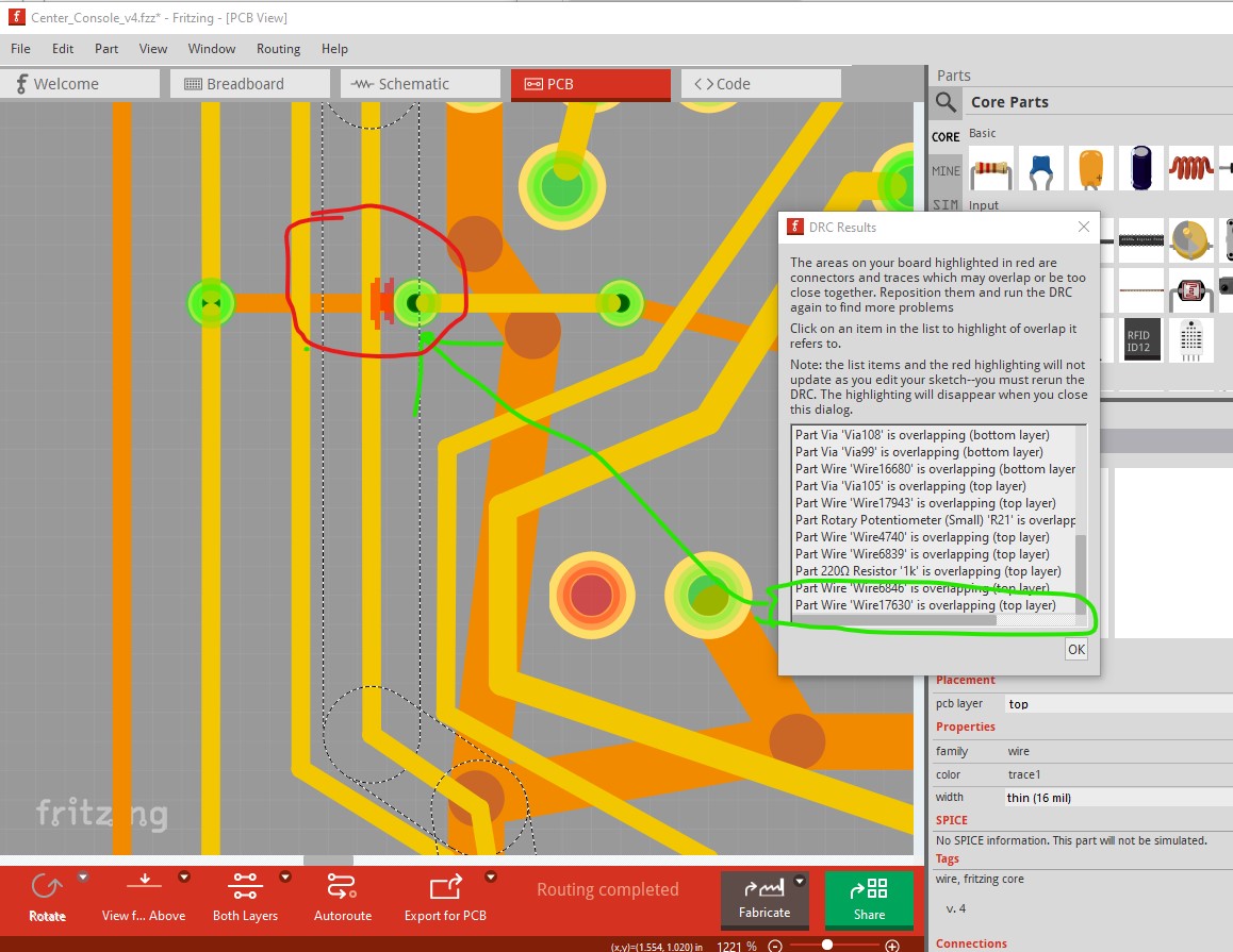
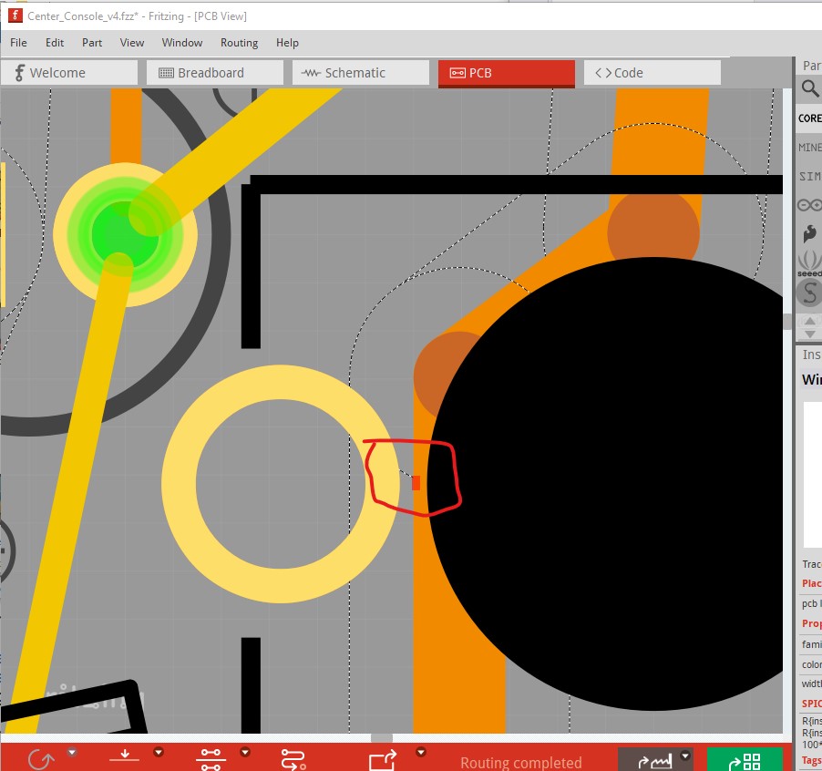
Routing->Design Rules Check creates this and is saying you have violated the default clearance rules in a variety of places. Clicking on a line in the DRC message should highlight the offending trace in pcb view (but doesn’t seem to be for me on 1.0.5 at the moment.) It is working now, so I did something wrong. Here is an example:
from the last wire in the list. As you see from the red on the trace the top layer trace is too close to the pad you need to move it left a bit (I suppressed the top silkscreen in View->Silkscreen top layer here to see better although that isn’t needed in this case). The rest will be similar (but sometimes are hard to find as the red can be quite small.) Snap to grid being on (you can set the grid size down if you need finer resolution) is a good cure for this. An unrelated suggestion is that it is a good idea to route schematic and check the results (I see it is currently unrouted.) It is very easy to make an error in pcb that will then reflect in to schematic and cause an unexpected connection. If the schematic it creates matches what you designed there is a better chance that it will work correctly. Hope this helps.
It is a bit odd that the ground fill doesn’t work even on simple examples. This feature is part of the test we run all the time. Are you using our official build?
I tried your sketch on Fritzing 1.0.5 and my dev build, both work fine.
About the next release:
I tested my current dev build with the sketch. Upcoming release 1.0.6 will show this warning: