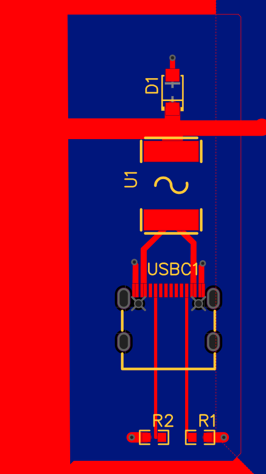
I designed a pcb with 60 leds, controlled by a ESP32. This is powered via an USB-C connector. I followed these instructions:
-
VBUS Pins (A4, A9, B4, B9) are joined and routed through:
-
A PTC fuse (MF-LSMF300/24X-2, C719172) for overcurrent protection
-
A TVS diode (SMF5.0A, C1509112) — cathode to VBUS, anode to GND — for surge/ESD protection
-
CC1 (A5) and CC2 (B5) each have a 5.1 kΩ pull-down resistor to GND to enable 5V output from USB-C
-
GND pins (A1, A12, B1, B12) are connected to a solid GND pour on the bottom layer
-
VCC (5V) is poured on the top layer, and GND vias are used to connect top-side components to bottom GND
My question is: are these instructions correct? And if so, can you judge from the image if I’ve correctly attached these components?
Thanks!!!