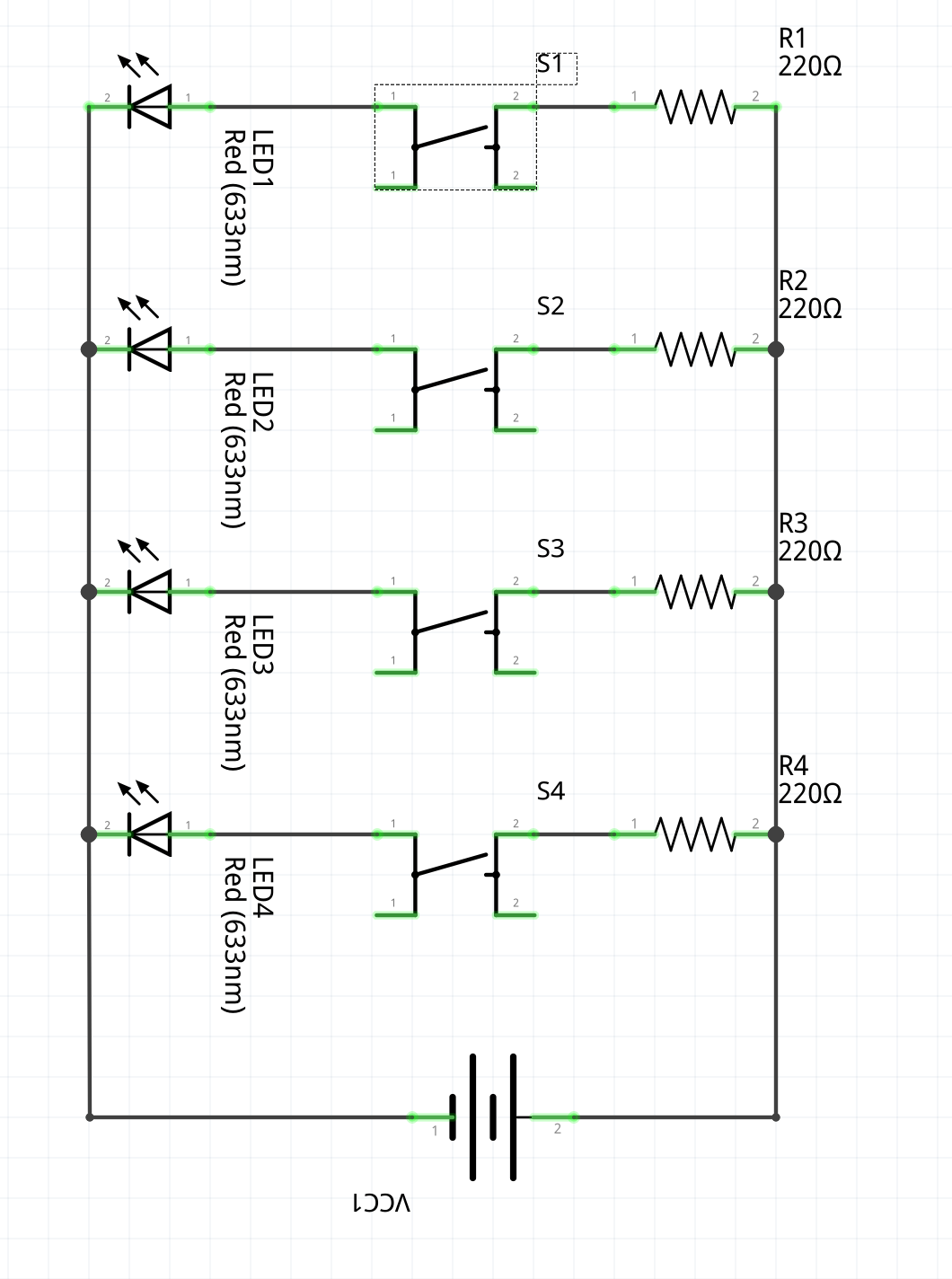
As this connection is not standardized (not like computer devices with IDE, parallel, …), the pinout of the cable and connector is chosen to make the pcb traces simple. This means, I can choose wire 1 for vcc and later, after progressing in the layout of the first card, move vcc to wire 2.
This pinout is constrained by the layout of the two cards which means a lot of back and forth…
The problem is when I change on a side it needs to change on the other side.
So far my solutions are not good enough. Do someone have ideas, experiences, … and recommendations ?
What I tested:
create a connector with “functional” pin. Then when I want to move the position of the wire, I just move the pin in the connector and reopen the sketch(es). That works great but it’s not a simple design process.
use net labels only on connectors and copy/paste the connector with net labels from board to board… that’s not efficient neither reliable.
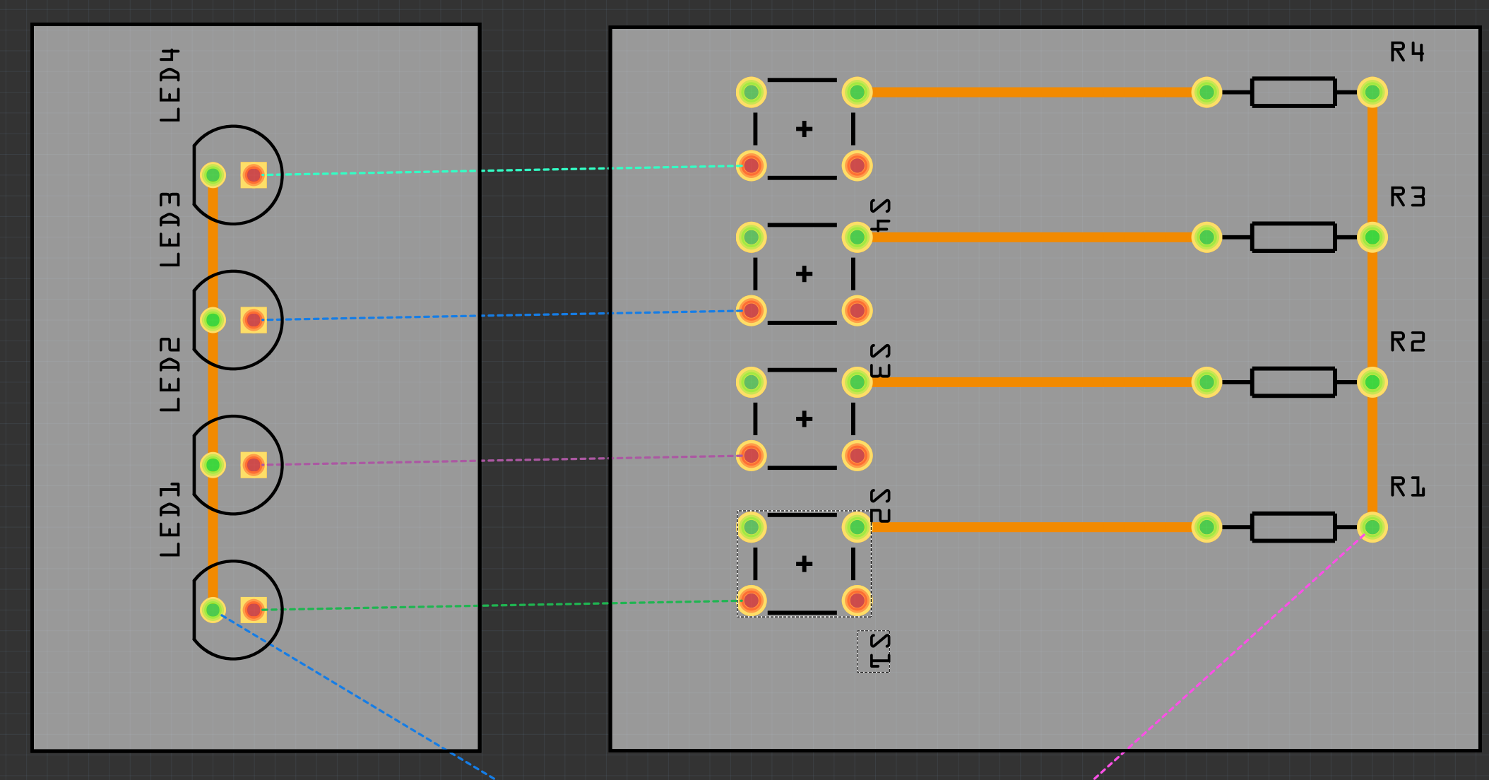
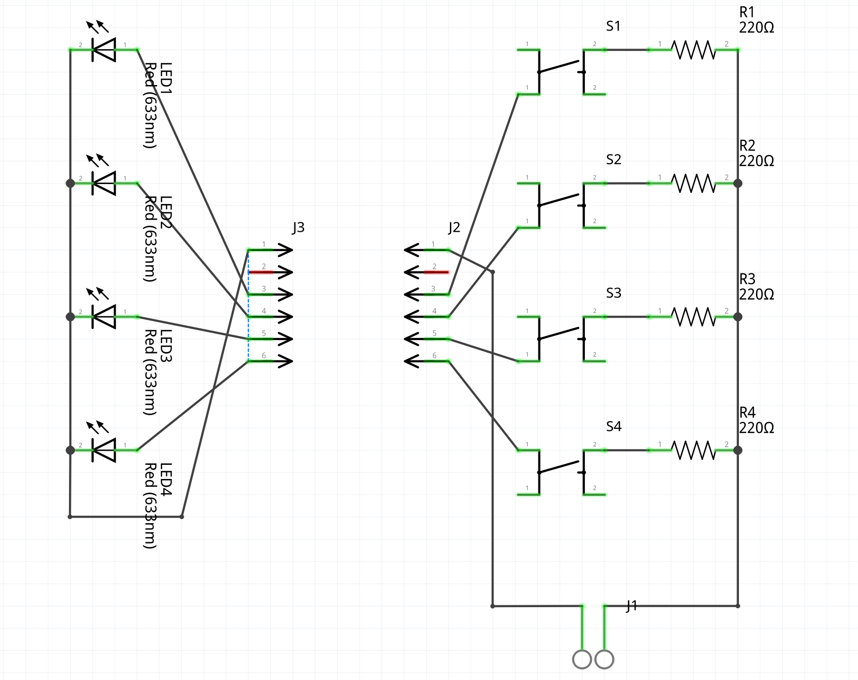
As you can see this change does not have effect on the left side. Because the left board is routed, when I move these connection, I would love to see dashed lines (unrouted), warning, … to do not forget to review the routing, on the second board. A bit like this:
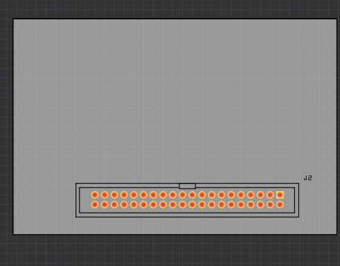
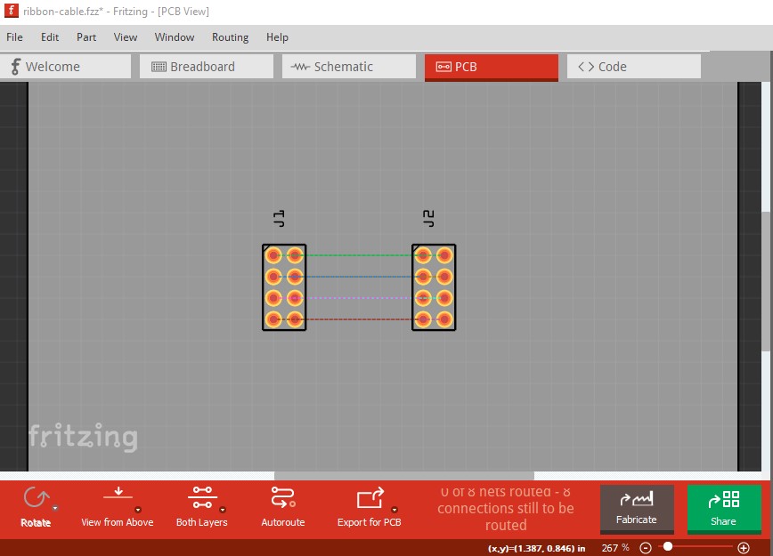
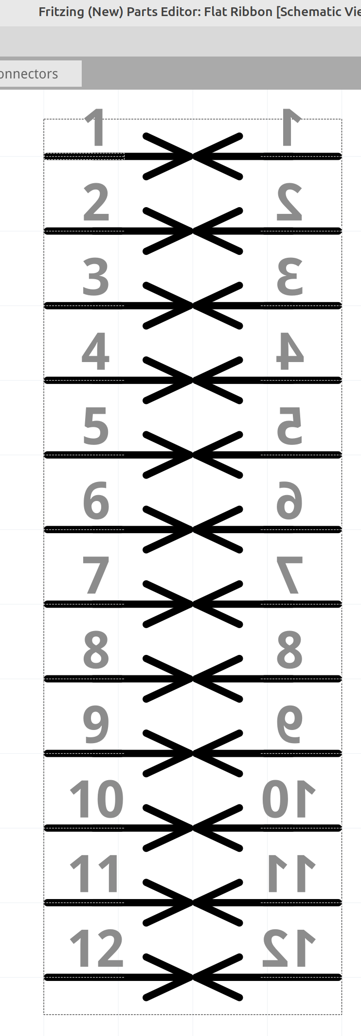
this ugly thing simulates the ribbon cable connecting two 8pin connectors. That causes rats nest lines to reflect in to schematic like this and tells Fritzing what the connections are so it can create rats nest lines for new connections (which I think may do what you want):
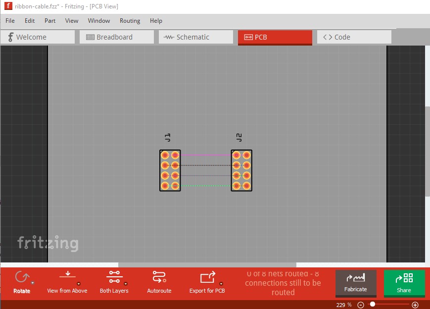
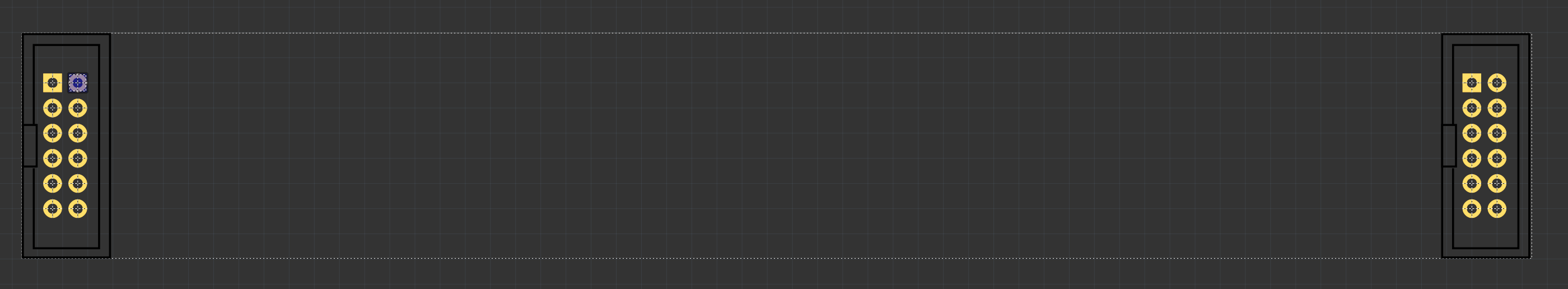
with that in place I think the rats nest lines you want should appear (because Fritzing is aware of the connections) the down side is that it only allows you to make the changes in 1 view (schematic or pcb) as the other view needs to be simulating the ribbon cable (the traces for which will be removed in the final sketch!) In this case pcb is simulating the ribbon cable allowing the changes to be made in schematic. If you now delete all traces in pcb (leaving the connections in schematic) you can change pcb to get the desired layout and the rats nest lines will reflect in from schematic:
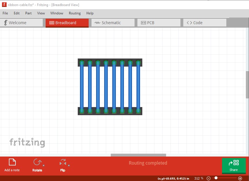
EditL I’m not thinking! The correct answer is to simulate the ribbon cable in breadboard, then the rats nest lines appear in both schematic and pcb which I think will do what you want.
Now if you make connections between the boards, the connections will light up yellow when clicked because the rats nest lines are reflecting in from breadboard. Updated copy of the sketch:
Please also note: It is common and perfectly fine to leave the connectors open in the schematic. This is a popular way to keep the schematics clean and readable.
Schematics can be separated into sub-circuits this way. A flat cable like you are using is a good natural interface where you could split the schematic.
If you see the connector symbol (the “Y”) and a label, like J1 above, then there is often a different page in the schematic, were the circuit behind J1 is described.
Thanks for these feed backs. To avoid messing up my cards, the only solution I found to modify the pinout on both sides is:
to have my own connector
to rename the pins
generate a new version of the part
remove the part from fritzing
close fritzing
open fritzing
import the new version of the part
reopen the sketch => automatically update the part and force me to reroute the pcb
This is a long scenario. Even if it works I use to do mistakes, forget, … and then half of my issues come from errors in connections…
BTW, Fritzing seems to be able to automatically update parts from github (never really saw it, a popup should say it ;-). If it could be possible to add my own repo, that would be so great !
Just for future reference, can you post the new version of the part and how you integrated it? Your scenario sounds indeed more complicated than it should be. We plan on improving Fritzing support for cables and connectors, and once we do, such information can be helpful.
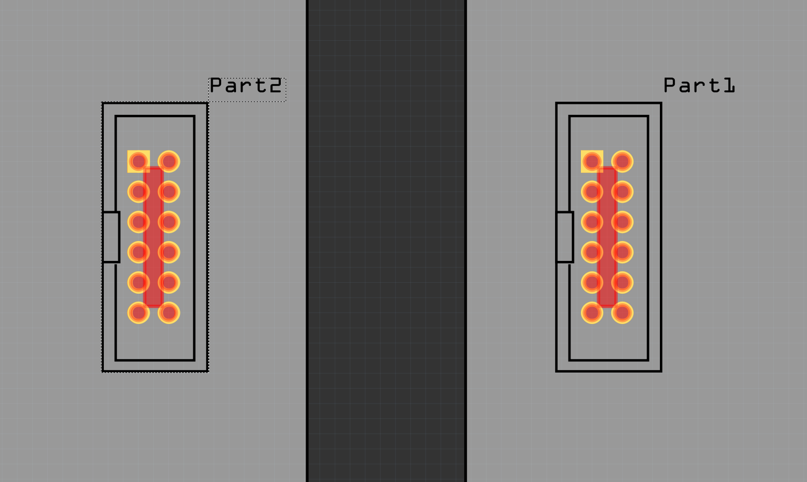
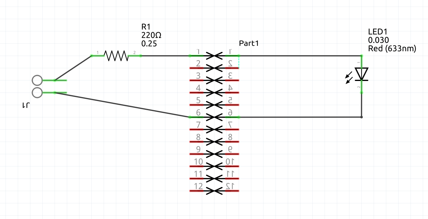
Flat ribbon connector
If you want to add a flat ribbon cable connector, for multi board sketch, I would suggest to create twin connectors and offer to add labels on pins. So in the sketch we’ll have this situation:
How twin connectors would work
In the Inspector of a connector we would have three additional widgets:
checkbox: to declare Part1 has a twin part
dropbox: to choose another part with same features to be the twin connector.
a textfield : to specify the order of pins ex: “pin0,pin1,pin8,pin2”. (not very user friendly, but maybe easy for a draft)
When a modification is made on a part, in the inspector, the same modification is applied on the twin part.
It would also be valuable to have functional labels on pins (vcc, gnd sda, …). Dynamically adding a textfield for each pin in the Inspector can be a solution… These labels might also be “net label” which can facilitate the schematic diagram.
NB: have twin part is maybe also applicable for other kind of parts.
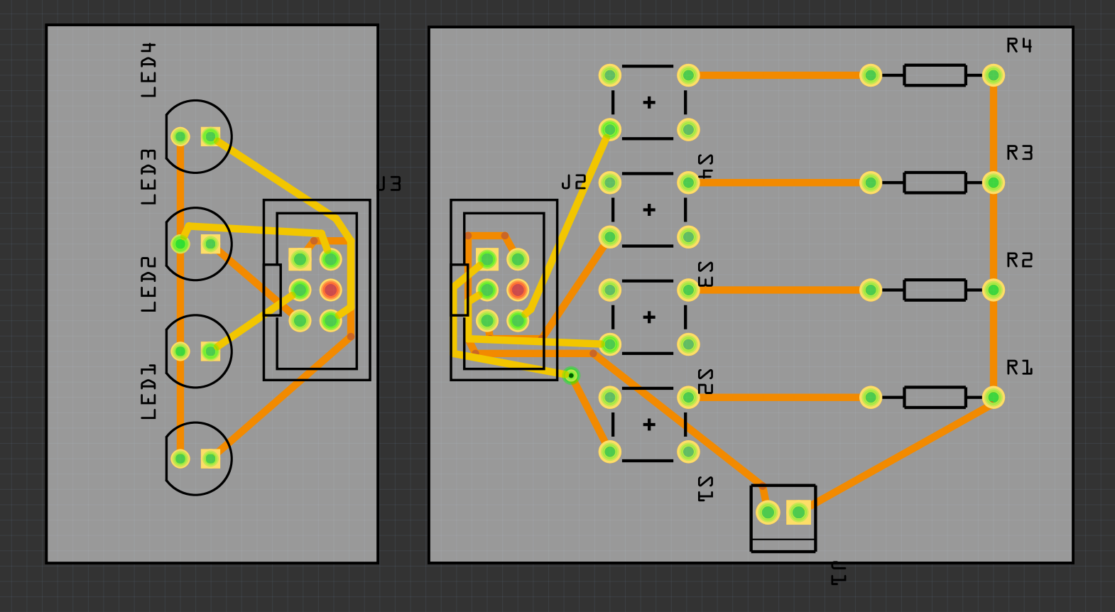
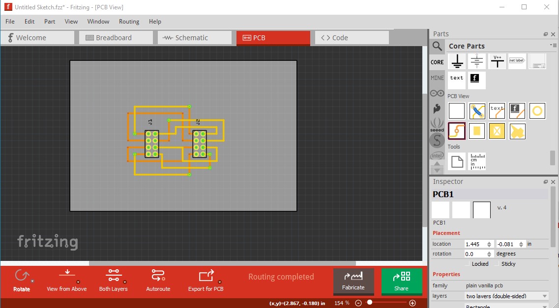
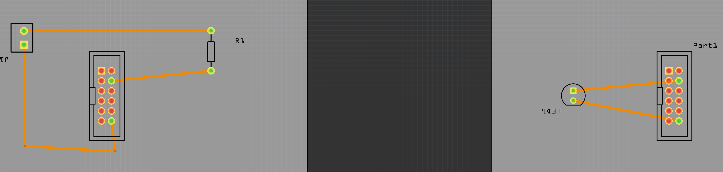
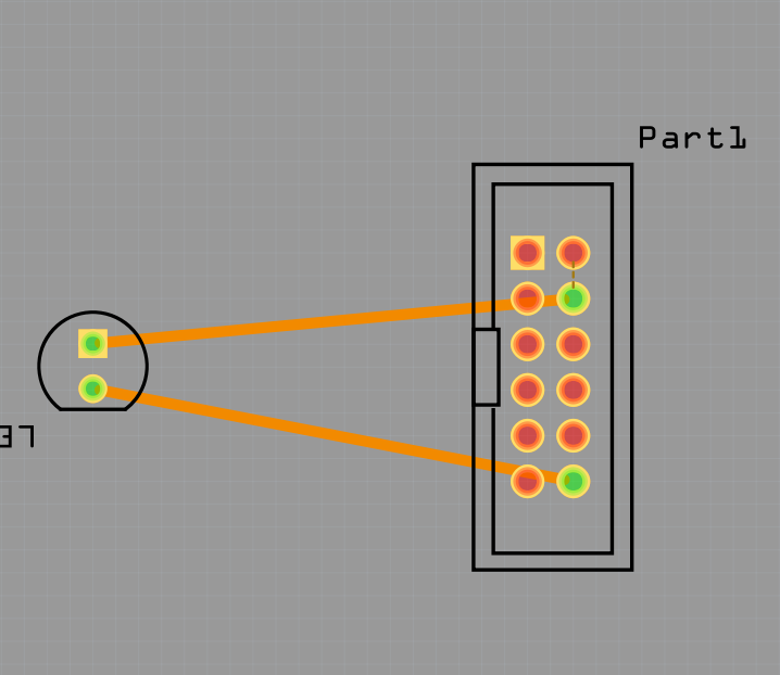
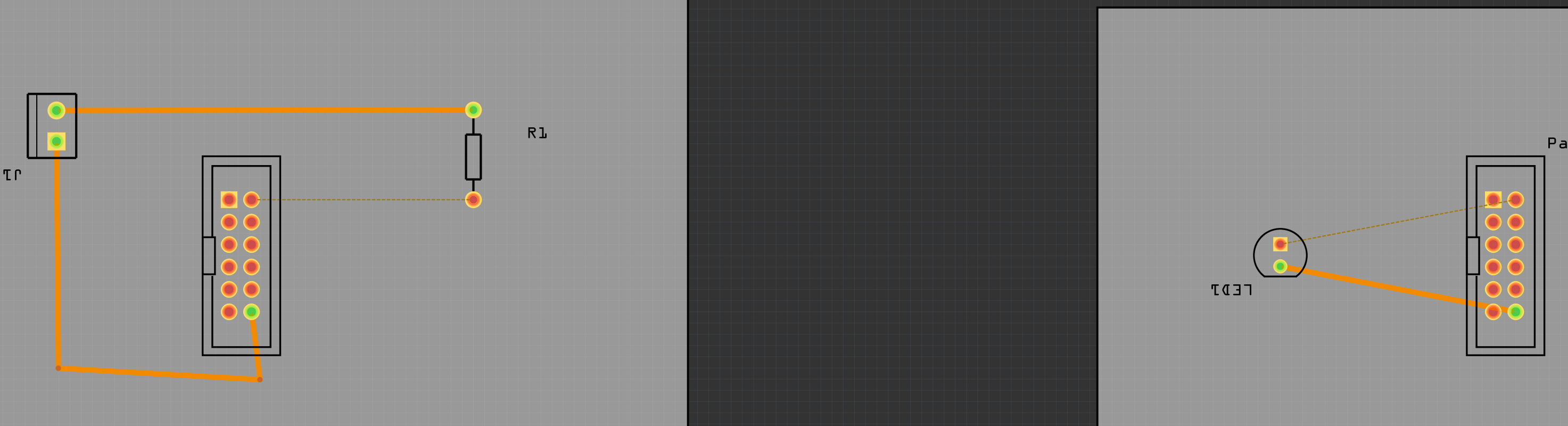
I went further on this topic. I’m now able to connect 2 boards in one single fritzing sketch, with a flat ribbon cable, which also support Gerber export for production.
This is a prototype which may need some graphical improvement.
The concept is to have 1 part with 2 headers and header’s pin are bused (very important).
Because the part is not as flexible as a real ribbon cable, moving the part on the first board moves it on the second board. This implies to position the “second” board regarding the second connector position (like moving a house relatively to the gate of the garden)
The distance between headers is fixed. This can be annoying if boards are too large.
Need to create one part per header pin count.
Need to have the same orientation for the two boards. So if we need to have two boards stacked in a box with a ribbon cable in the middle, we need to make a variant to flip the headers.
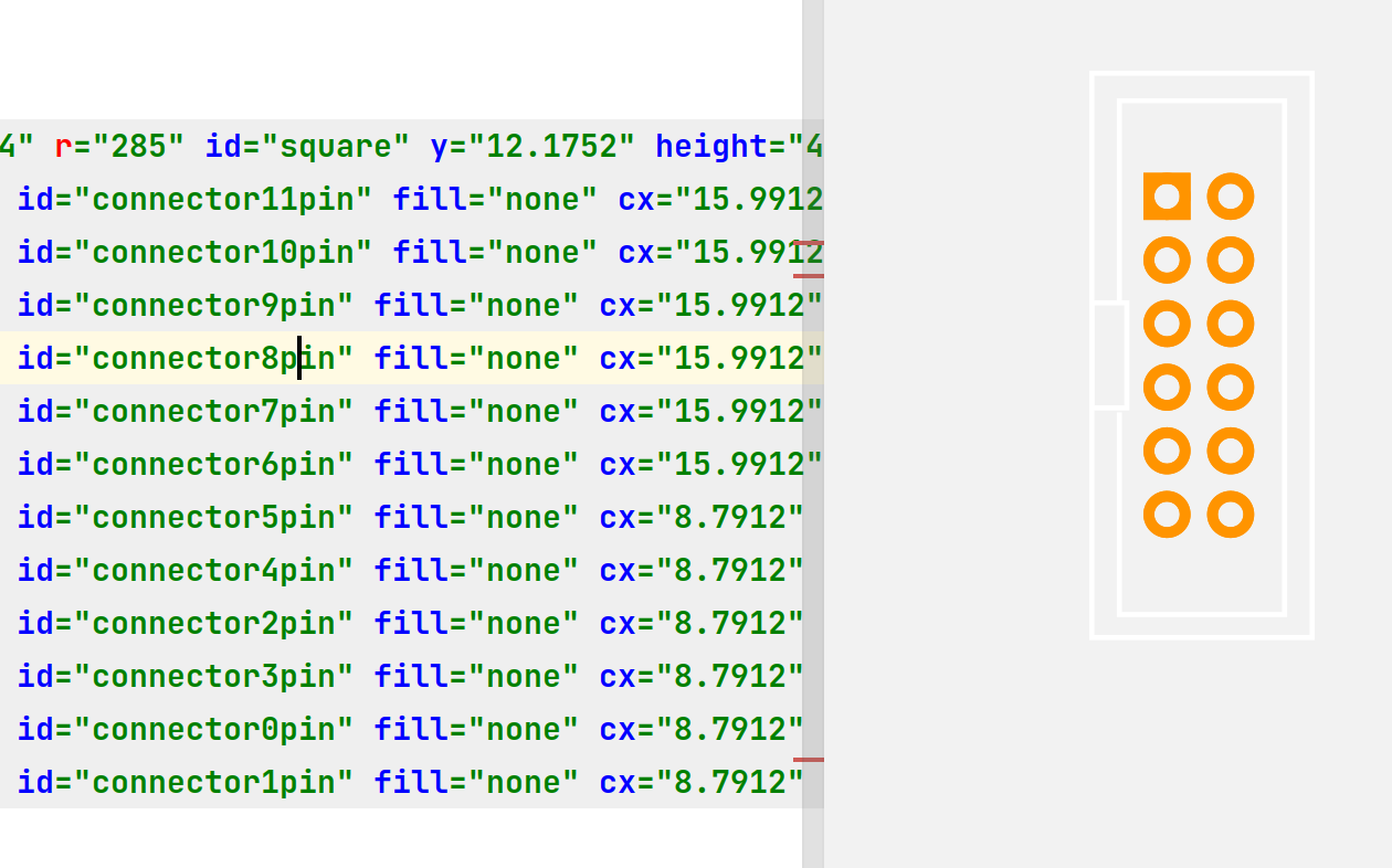
Appears to work about as well as it can given the Fritzing limitations. The fzp file needs a label of J to give it a J# type part label is the only thing I see. Part1 comes from no label element in the fzp file.