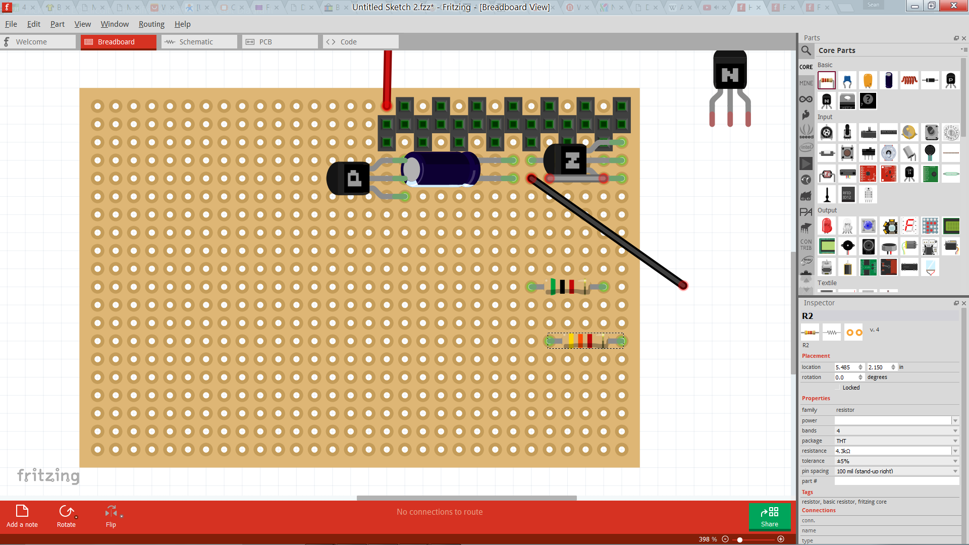
I’m planning a circuit to go into perfboard. How do I access the other side of the board to plan the rows of pins that will be bridged with solder? My searches suggest it’s possible but give no information on what to click on to make it happen.
You got me there.
The pref board only appears on the breadboard view, and I don’t think you can double load a board there - there would be a button on the bottom red bar, like in PCB view, to look at it from the other side -.
I suppose you could just put links on the top and remember to put them on the bottom.
Maybe you could use PCB view with the grid set at 0.100" and manually put in tracks top and bottom. Top tracks are yellow and bottom are orange.
I can’t make any sense of PCB view. PCB view bares no resemblance to the arrangement of parts I have on the perf board. Fritzing doesn’t really seem to be design with perf board in mind. How do you put links? Do you mean wires? The holes are already occupied by parts so can the links occupy the holes at the same time as the parts?
Go to View/Set Grid Size and enter 0.100". Each light grey grid intersection is where a prefboard hole is.
Click on grey PCB and in Inspector change the size to what you want.
Put the parts in the same position as on the prefboard, and click on a parts connector and drag it to the other parts connector. If you waant 90º links just grab a track in the middle and drag snap it to a grid.
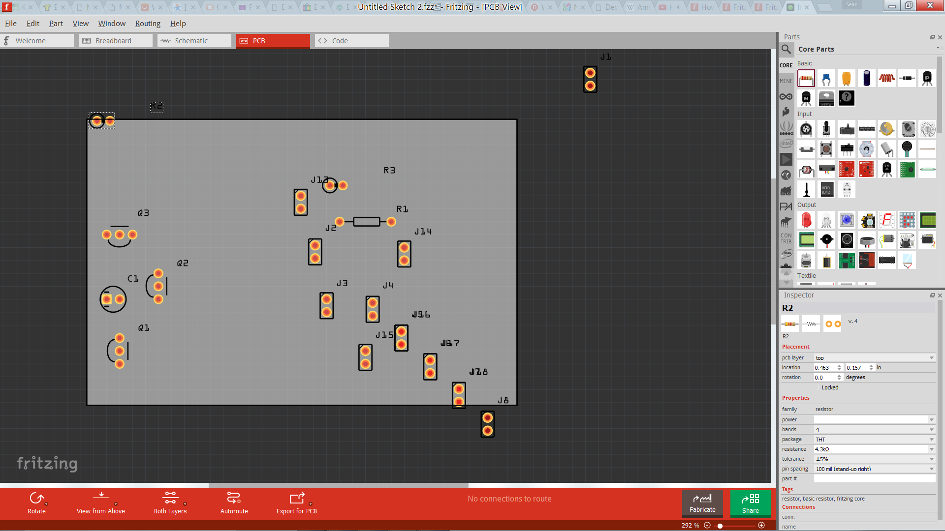
Why aren’t the parts in the same place on the PCB automatically? They’re positioned randomly. It looks like pin spacing affects the PCB view but not the breadboard/perf board view.
Yeah I know. That pretty much happens in all the other views.
The parts in BB view are dimensionally accurate engineering drawings where as the BB view are representative, so accurate positions might not be the same.
I suggest you Print Screen and have the pic open next to it as a reference…
I just though, you could get a via in PCB view and resize it to a prefboard connector, press copy, and the CTRL+D 100 times, and then drag them to each intersection to make a prefboard in PCB.
Get a what in PCB view? I think that’s a typo!
Got to the bottom of Core parts, category PCB View, and drag a VIA onto the PCB.