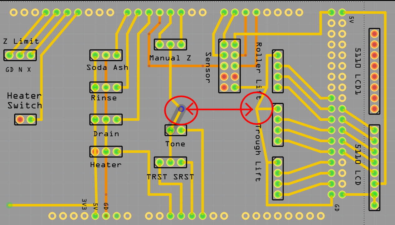
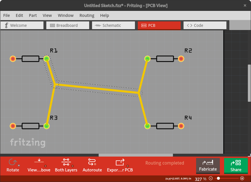
How do I connect the two traces at the points shown? (They’re just bent like that to clarify what I want to connect.)
Connect two of the pads to each other then drag the trace where you want it.
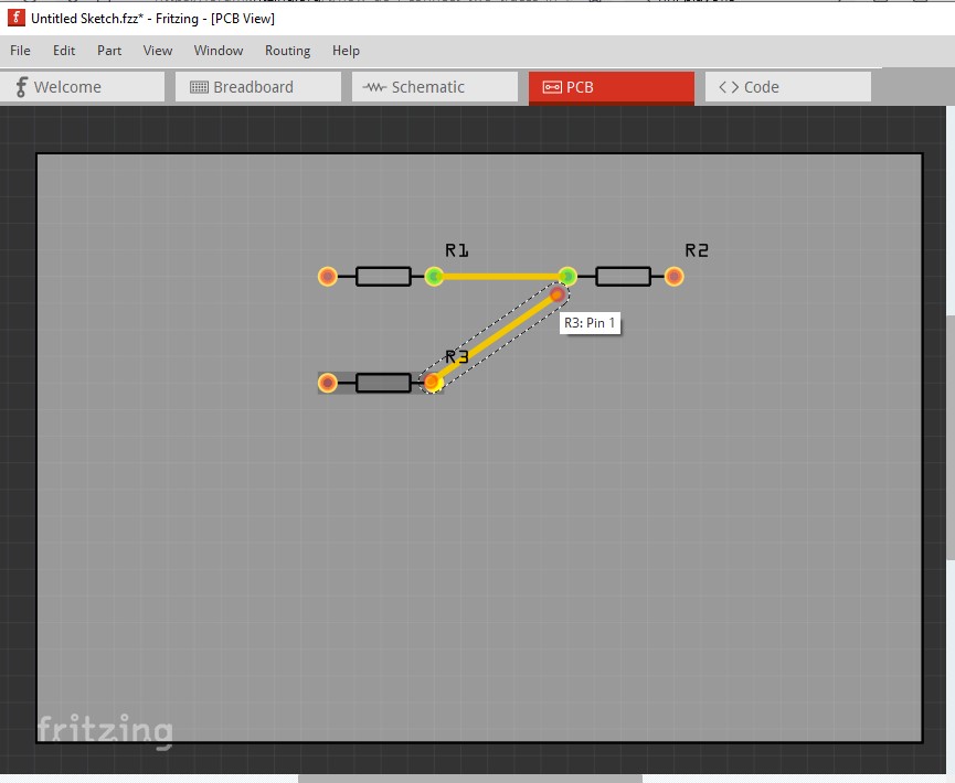
finish the connection by dragging it to the pin on R2 then drag the trace to line up how you want.
Peter
Starting from your example, with 2 separate traces that you want to connect, here is one way to do it.
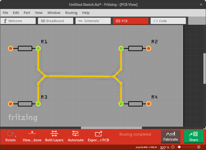
- add an extra bend point to one of the existing traces
- right click on the new short segment, and select “Delete Wire up to bendpoints”
- add another bend point to one segment of the now broken traces
- move the open end of the other segment onto the new bend point
- move the remaining open end to the bend point in the other trace
- move and add bend points to get the routing you want


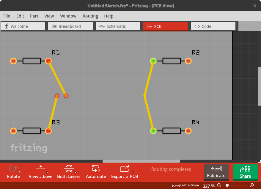


When one of the existing traces is ‘simple’, it can be easier to delete that trace (say between R1 and R3). For that:
- create trace from (say) R1 to the bend point in the trace between R2 and R4
- drag a bend point in that to where the intended connection point is wanted
- create trace from R3 to that bend point.
- finish the routing of the trace segments.
@vanepp I think your version results in a trace laid on top of another trace. That works, but means extra work to make sure any future changes keep the traces lined up. What I did does not have any overlapping traces, and moving the intersection points in the traces brings all of the segments along.
A warning for my version. I have had ‘glitches’ when joining more than 3 traces at a single point that way. It might be better (safer) to add a pcb “Pad” part where you want the join, then bring all of the traces to that. The effect should be the same. Just make that pad the size of (or smaller than) the traces. Moving the pad will bring all of the connected traces along.
RE: pcb pad. Can you post a screenshot of what you mean?
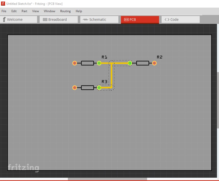
The pad is the end of the resistor. In the first screen shot I started at the red dot on R3 (which is what I called the pad) and extended the trace to almost the connect point on R2 before taking the screen shot. I then completed the connection from R3 to R2 and bent the resulting trace to get the desired routing. That said, @microMerlin 's way is probably the better way (if more complex and I am usually lazy) to do this, since as he notes you have to move both traces to move the join point in my method.
Peter
In the PCB view of Fritzing, in Parts window, scroll almost to the bottom. In the section “PCB View”, there is a part named “Pad”. Once placed in the view, it’s size can be changed, either by dragging on the corners, or by using dimension options in the Inspector window.
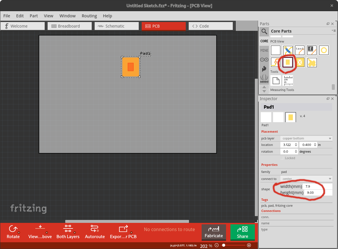
Note the pad is SMD (it exists only on the top or bottom of the board) so you won’t be able to change sides of the board with the traces (they will only route on the top or bottom depending on which side the pad is on.) I point this out because this bit someone else recently.
Peter
OH. Cool. And I can upload that to Aisler? Is that a “component” that has to be assembled, or just the PCB just come with?
@vanepp I deliberately choose a pad because of that. A trace is always only on a single side of the board. If you want to (also) connect to a trace on the opposite side of the board, use a via instead.
The thing to watch, is that if you want to move the traces to the other side of the board, you also (maybe first) need to move the pad to the other side.
@billTheTailor The pad is only copper on the PCB. There is no component to be assembled. It should export (to gerber) the same as any other section of the copper traces. If Aisler is processing a Fritzing .fzz file directly (I have no information about that), a quick test to verify they see the pad as copper might be good. That pad part is also used to create ‘fingers’ to use for connectors at the edge of the PCB.