My First part creation:
Heltec LoRa node 151 a Low Power board with STM32L and SX1276.

Heltec_LoRa_node_151.fzpz (48.8 KB)
My First part creation:
Heltec LoRa node 151 a Low Power board with STM32L and SX1276.
Heltec_LoRa_node_151.fzpz (48.8 KB)
I ran the contents of that part file through FritzingCheckPart. Here is a summary of what it reported, and what I noticed doing a manual inspection and smoke test in Fritzing.
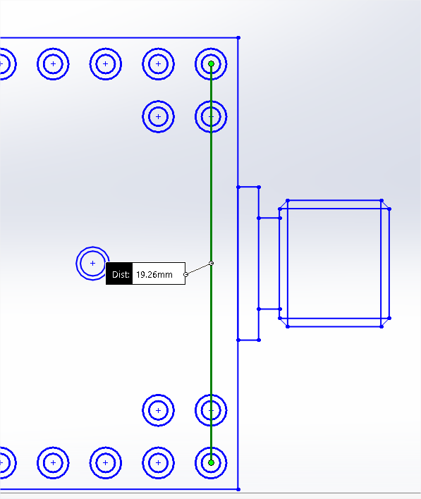
I did not look for the datasheet for that board, but I see something that looks unusual. The header pins appear to have the standard 0.1 inch spacing on breadboard and pcb view, but the distance between the outer rows of pins is not a multiple of 0.1 inch. It seems to be about 0.73 inch. Is that correct?
The antenna connection appears to not be quite centered between the outer pin header rows. That could be where the offset noted above comes from. If the bottom row was moved up slightly, I think it would both align to the 0.1 inch grid, and bring the antenna connector to the center.
There are ‘px’ units on font-size attributes in the breadboard and schematic view svg files that Fritzing is known to not handle well. The text size can change from what was intended. Fritzing wants just numbers, without units. Using ‘px’ units is valid for the svg format specification, but Fritzing does not handle it. Visually, in Fritzing in my environment (Fedora, Fritzing 0.9.4), some of the breadboard text is very small, as is all of the label text in schematic view.
The pcb view schematic has some silkscreen graphics with the fill color set to “#ffcc00”. It appears that these are all straight lines, where fill does not do anything, but the color should still be set to “#000000” (black) to match the rest of the silkscreen.
The part definition file (fzp) is missing a fritzing version attribute in the module element. I am a bit surprised by this one. From other information seen, it appears that this was generated from the generic IC, and I would expect that Fritzing would automatically include a version number with that. Perhaps the “parts factory” code is missing the version number. Adding fritzingVersion="0.9.4" in the module element will fix this one.
The part definition shows terminalId attributes for connectors in the breadboard view, which do not actually exist in breadboard svg. If the terminalId is defined, a matching graphic element should exist in the svg. terminalId entries are not typically needed for breadboard view.
The part definition shows terminalId attributes for connectors in the schematic view, which do not actually exist in schematic svg. These should exist in the svg. They are used to give Fritzing a reference point, to “snap” wires to. Without this, wires attached to the connectors will be drawn to the middle of the connector pin line, instead of to the end.
Warnings are being reported about “-inkscape-font-specification” attributes with invalid values. As long as the standard svg “font-family” entry also exists (they seem to), the inkscape specific extension can be safely ignored.
The “silkscreen” layer (group) in the pcb schematic should be above (before) the copper layers. That makes selecting things in Fritzing a bit easier.
In the svgId “connector«number»pin” values, the “number” should be in ascending sequence starting with “0”. Without any gaps. This part as a “connector27pin”, then a “connector47pin”. The 47 through 54 pins should be renumbered to 28 through 35, in the fzp file, and all of the svg files. That will affect the terminalId (connect«»Terminal) entries as well.
The “schematic” layerId specified in the fzp part definition does not exist in the matching svg image. This will “appear” to work in Fritzing, but exporting a sketch to an svg image will not include the part. The “schematic” id should be added to the first/outer wrapper group element.
The family for the part is current “Generic IC”. That should probably be something like “LORA” (or “LoRa”). The taxonomy field shows “part.dip.28.pins” this is not a dip package. If no “good” value can be figured out, remove the taxonomy entry completely.
The label for the part should be something short like ‘Mod’. Without any number at the end. This is used by Fritzing as the default prefix, with a number appended, to create a unique identifier in sketches. To tell part instances apart where there are multiple copies in the same document. The current label, “Lora_node151”, becomes “Lora_node1” for the first copy of the part, then “Lora_node2” for the next. The initial number suffix is removed, then 1, 2, … appended to create the actual (initial) part label.
The part graphics for the schematic view is offset from location of the actual connector lines. By about 4.4 inches one direction, and 5.4 the other.
The connector lines in the schematic view should be (by standard/convention) 0.1 in long. Many older parts do not follow the latest rules. There does not need to be a large gap between the (upper and lower) end pins and the edge of the body of the board graphic. 0.05, or a most 0.1 inch is enough.
The schematic view svg has been created using “mm” as the units. That works, if other things are done correctly, but it is more usual to use “in”, since the connectors are (typically) supposed to align to the 0.1 inch grid.
Hello microMerlin, and thanks to take your time to check what i’ve done
for the placement in PCB view i take the dimension in this file http://resource.heltec.cn/download/LoRa_Node_151/LoRa_Node_151.dwg
That drawing does not actually show the dimensions between the outer rows of pins, but a dimensioning tool reports that it is 19.26mm, which is about 0.758 in. So that really is not on the 0.1in grid. That does not match my 0.73 in either though. I got that using the ruler tool in Fritzing. Maybe I miss-used/miss-read that, but it needs confirming. You should print out a sketch with the part at 1:1, and verify that the holes line up accurately with a physical part.
I checked with Solidworks to evaluate dimensions in dwg files and 19.26mm is the correct spacing (with the real board i have approximately the same dimension.
I hope this version is better 
Heltec_LoRa_node_151.fzpz (49.1 KB)
I ran the contents of the new version of the part file through FritzingCheckPart. Here is a summary of what it reported, and what I noticed doing a manual inspection and smoke test in Fritzing.
In the fzp file, the svgId for the schematic layer of connector28 has a typo. It is currently “connector2/pin” instead of “connector28pin”. The same error is in the svg file. Since that is just a text key for Fritzing to match with, it should work fine as is. FCP complains because it does not match the standard pattern, with the prefix for the svgID matching the connector id.
The fzp file is missing terminalId attribute values for connector28 through connector35. The elements do exist in the svg file. For example:
<schematicView>

<p layer="schematic" svgId="connector29pin"/>

</schematicView>
should be something like:
<schematicView>

<p layer="schematic" svgId="connector29pin" terminalId="connector29terminal"/>

</schematicView>
The breadboard svg has conflicting font information. Elements have a “font-family” style of “OCRA”, but the “-inkscape-font-specification” style is ‘Droid Sans Italic’. Fritzing does not recognize the inkscape extension, so OCRA is being used, not Droid Sans.
The schematic view connector terminal (rect) elements have a zero width, which means they are not selectable (graphically) in Inkscape. They should have a small width and height (usually a square) that is centered around the connector snap point (the end of the connector pin line). For example:
<rect stroke-width="0" id="connector35pin" height="9.7222" y="95.1389" gorn="0.2.93" fill="none" x="800" connectorname="VDD" width="200"/>

<rect stroke-width="0" id="connector35terminal" height="9.7222" y="95.1389" gorn="0.2.94" fill="none" x="1000" width="0"/>
could be
<rect stroke-width="0" id="connector35pin" height="9.7222" y="95.1389" gorn="0.2.93" fill="none" x="800" connectorname="VDD" width="200"/>

<rect stroke-width="0" id="connector35terminal" height="2" y="94.1389" gorn="0.2.94" fill="none" x="999" width="2"/>
The “silkscreen” layer (group) in the pcb schematic should be above (before) the copper layers. That makes selecting things in Fritzing a bit easier. This has not changed from the previous version.
The “breadboard” layerId specified in the fzp part definition does not exist in the matching svg image. This will “appear” to work in Fritzing, but exporting a sketch to an svg image will not include the part. A wrapper group element (for the whole svg image) needs to be added to the svg file, with the id set to “breadboard”.
The part definition still shows terminalId attributes for connectors in the breadboard view, which do not actually exist in breadboard svg. If the terminalId is defined, a matching graphic element should exist in the svg. terminalId entries are not typically needed for breadboard view. For example
<breadboardView>

<p terminalId="connector0terminal" layer="breadboard" svgId="connector0pin"/>

</breadboardView>
should be
<breadboardView>

<p layer="breadboard" svgId="connector0pin"/>

</breadboardView>
FCP is complaining that it found a drawing element before a layerId (or no layerId) for the pcb svg file. In this case, it is because both the copper1 and silkscreen groups (layers) are themselves wrapped in 2 other groups with a transform. That can be fixed by (in Inkscape), selecting that outer group, and doing an ungroup 2 times. That is 2 times for the group around copper1, and 2 times for the group around silkscreen. That should leave the copper1 and silkscreen layers as “top” level elements in the svg file, with the transforms on them.
The connector20 entry in the fzp file has a terminalId entry fo the copper1 layer of pcbView. As for the breadboardView, the terminalId attribute should be removed.
The connector pin line graphics in the schematic SVG are still 0.2in long. They should be 0.1in.
This is not a “problem”, but the id values for bus entries in the fzp file could be given descriptive names. Instead of “internal1” and “internal2”, “GND” and “VEXT” are perfectly valid. Or “ground” and “external voltage”.
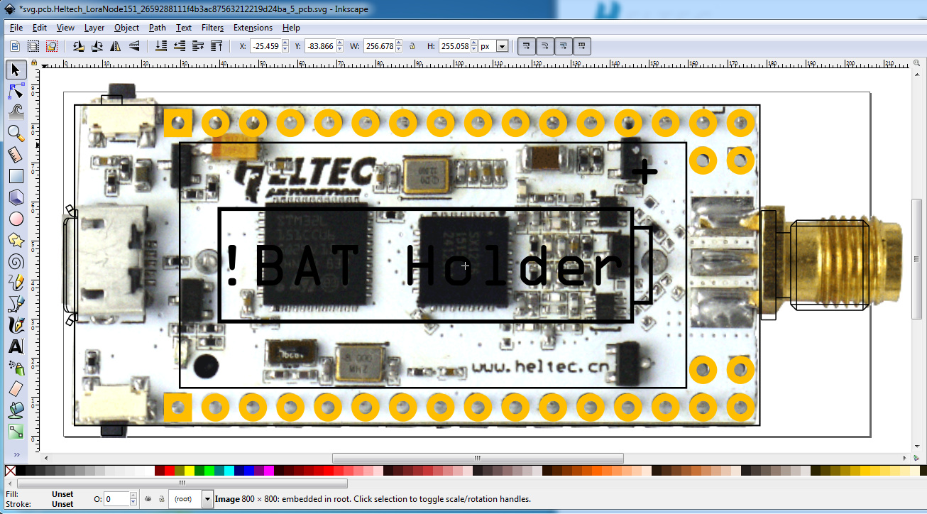
Did you intend to include a battery holder as part of the silkscreen for the pcb svg? That might be the location used for your (current) project, but is that really expected for all usage of the LoRa board? I would keep the part as standard / generic as possible, to not include anything the might not exist for an individual projects. Extra parts can be added in in a Fritzing sketch, they can not be removed without recreating the part.
I expect this is correct and intended. I grabbed a jpg of the board from the heltec site and imported it in to Inkscape then scaled and skewed it and overlayed it on the pcb svg and the holes appear to match up:
However checking a real board against the pcb layout printed at 1:1 scale would be the correct thing to do since this method is not particularly accurate …
The reason for the not .1in spacing is so that you can not plug it in to a breadboard. If you do so the pins circled in red will short as we see here:
and may damage the board. So they look to have made it so it can’t plug in to a breadboard. That said, I see a number of issues here, the most important one is that the pcb hole size is 0.035 in (because this was cloned from a generic IC) and needs to be 0.038in to fit a .1 header if desired. To change hole diameter from 0.035 in to 0.038in to fit a .1in header the easiest way is to edit the pcb svg with a text editor and change the radius on all the holes from 27.5 to 29:
from
   <circle
     transform="rotate(-90)"
     id="connector0pin"
     cy="305.94022"
     cx="-842.85913"
     gorn="0.3.0.0.0.5.0.0.0.0.0.0.0"
     r="27.5"
     style="fill:none;stroke:#ffbf00;stroke-width:20" />
which generates a 0.035in hole in the gerber drill.txt file:
Untitled Sketch_drill.txt
; NON-PLATED HOLES START AT T1
; THROUGH (PLATED) HOLES START AT T100
M48
INCH
T100C0.035000
%
T100
X008146Y014651
to
<circle
  transform="rotate(-90)"
  id="connector0pin"
  cy="305.94022"
  cx="-842.85913"
  gorn="0.3.0.0.0.5.0.0.0.0.0.0.0"
  r="29"
  style="fill:none;stroke:#ffbf00;stroke-width:20" />
and
; NON-PLATED HOLES START AT T1
; THROUGH (PLATED) HOLES START AT T100
M48
INCH
T100C0.038000
%
T100
X022509Y014088
In Inkscape the hole diameter is set by
hole diameter = pad diameter - (2 * stroke-width)
for a 0.038 hole the pad diameter needs to be 0.078in with a stroke width of 20 (at 10.41667 scale.)
I rescaled the breadboard svg to be the recommended 10.41667 scale (1 drawing unit = 1 thousandth of an inch.), regrouped it and added the breadboard layerId. As well I changed the pin numbers so the extra 4 connectors at the antenna end of the board are in their own groups as in the official schematic.
schematic:
It was easier to make a new schematic from the template than fix all the faults in the original (the parts factory currently generates svgs which don’t meet the graphics standards.) I changed the labels from the cpu pin number to those in the official schematic at
If that doesn’t suit you feel free to change them back. The terminalIds are all set correctly as part of the rebuild (I have tools which do so.) If you make changes in Inkscape you either need to run it through FritzingCheckPart.py or edit the svg and remove the px from the font-size which Inkscape will add. Fritzing objects (and will set the font size to 0, erasing the text) under some circumstances.
pcb:
Mostly the radius change for the hole size, but I also removed an unused def which will have caused FritzingCheckPart to complain about the layerIds (a bug in FritizngCheckPart that I haven’t fixed yet.) All these changes are contained in this part:
Heltec_LoRa_node_151-improved.fzpz (26.4 KB)
Yes, the battery holder is part of the heltec module itself not an add on. It isn’t clear from the picture that the pins will reach the pcb with the battery present though (although extra long headers like used with the arduino on the pcb would probably work.) As well the pins that would short are not installed in the photo, so I’m not sure why they didn’t make it breadboard friendly.
Peter