Heltec Dev Boards

it would be nice if you can change the holes to 1.447mm/0.058, I will do a prototype test for you and confirming the outcome for the good use of everyone.

I am limited to 3 replies only so I reply here:

Excellent, I will send it for production it will take a week more or less :slight_smile:

Ordered, I will get you posted with information and pictures if it fits

See how you go with this one (pads 1.447mm/0.058in).

Amica_NodeMCU_DevKit_1.0 (v2).fzpz (56.8 KB)

1 Like

The problem is that the svgs are dimensioned in px and thus the gerber export is the incorrect scale. I’ll correct that and post a corrected version in a bit. The holes in the pcb are not on .1in centers due to the incorrect scale.

Peter

Thanks @vanepp.

As you know, I use Illustrator to prepare my files, and we’ve encountered this problem before [in a slightly different context]. Having now looked a little more deeply into this problem, one solution that’s been suggested is to simply change the ‘px’ unit (which, in Illustrator, is 1/72") in the SVG file to ‘pt’ (which, I believe, is universally recognised as 1/72"). The files open OK, but I can’t quickly see if the that fixes the present problem.

@vanepp, I’ll be very interested to see what you come up with. Changing the units to ‘pt’ doesn’t seem to make any difference (you’ll probably know immedaitely why that is).

As best I can determine from the Gerber files, though, the drill hole being specified [for my original part] is 28 mil, which on boards that I have at hand seems to take a normal pin header snugly, but without needing any force—I do normally specify a drill size of 1mm (~40 mil) for a header pin (the drill holes generated for the larger pads I created in the above part are ~41 mil), but there’s plenty of ‘spare room’ in those holes.

The variation in the separation between holes only appears to be in the fourth decimal place (i.e. a tenth of a mil), which I would have thought would have little impact.

Yes, the problem is that you need to change the drawing units from px to in. As part of that Inkscape redoes all the internal sizes. I don’t know of a way to do that in Illustrator, reading their documentation I’m not sure it is possible (although Illustrator appears to process a svg that is dimensioned in inches just fine.) They seem to think they know best and you should just use what they give you (although there may be some way I don’t know to set the values as well.) Here is a fixed up version of the part and what I did to get there. Since I was doing it anyway I converted everything to meet the graphics standards as well as fixed the pcb svg.
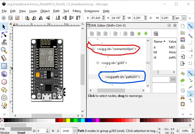
breadboard:

Mostly just rescaled this so 1px = 1 thousandth of an inch. In Inkscape this is described here:

again I don’t know how (or if!) this can be done in Illustrator. As well the connector0pin is set as a group rather than on the path drawing element, since I needed to ungroup the svg to rescale it, I moved connector0pin to the path.

Schematic:

Changed the line colors to match the graphics standards and changed the terminal definitions to a 10 thou by 10 thou rectangle.

pcb:

FritzingCheckPart.py complains about the drawing units being px (which can cause scaling problems):

Warning 19: File
‘svg.pcb.Amica_NodeMCU_DevKit_1.0_pcb.svg.bak’
At line 4

Height 134.363px is defined in px
in or mm is a better option (px can cause scaling problems and likely did here from the example board above!)

Warning 19: File
‘svg.pcb.Amica_NodeMCU_DevKit_1.0_pcb.svg.bak’
At line 4

Width 70.3px is defined in px
in or mm is a better option (px can cause scaling problems!)

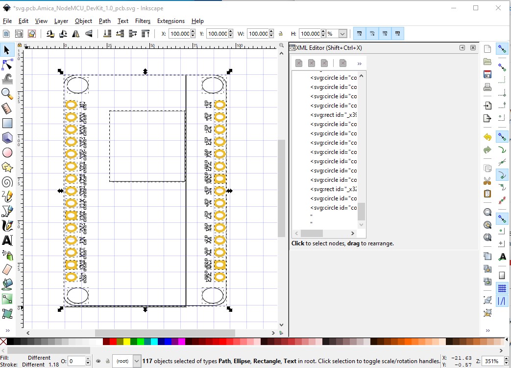
This corresponds to this in the xml (and in Inkscape):

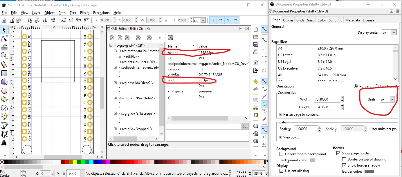
The red circled height and width in the first line of the xml are the problem. If defined in px, then Fritzing guesses which of 72dpi or 90dpi was used on the original and sometimes gets it wrong (especially now when the newest svg standard is 96dpi!) As we see in this image the pins are not on .1in boundaries (because this Inkscape is using 96dpi.) The blue grid lines are on .1in boundaries. So I figured out what they should be and scaled them to that. X pad to pad distance should be 0.9in, currently they are 0.671in,

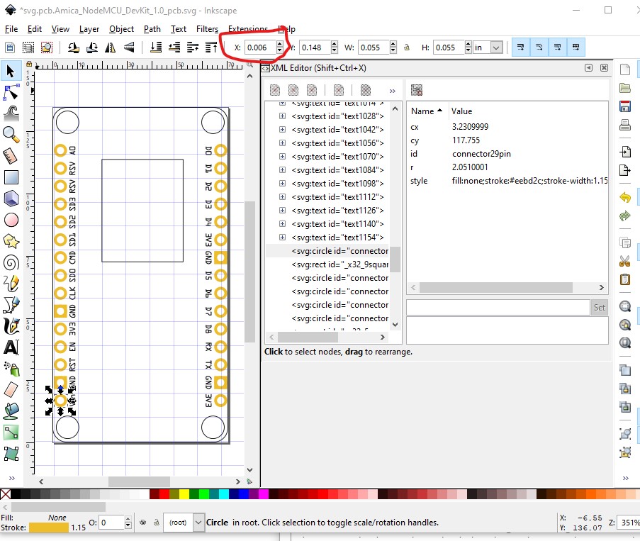
determined by setting dimensions to in and selecting the bottom left pad with a X offset of 0.006in and then the right bottom pad:

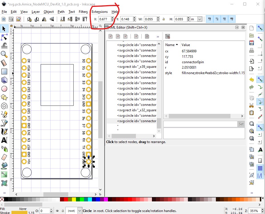
which is at 0.677in (but should be at 0.906in!) So scale up by 1.341281669150522 in x by setting the width from 100% to 134.1281669150522%

Which widens the X dimension (while distorting the Y as we haven`t changed it yet!) so that the pads are now spaced exactly 0.9in apart as desired. Now do the same in the y (height) direction changing height from 100% to 133.8432122370937%.

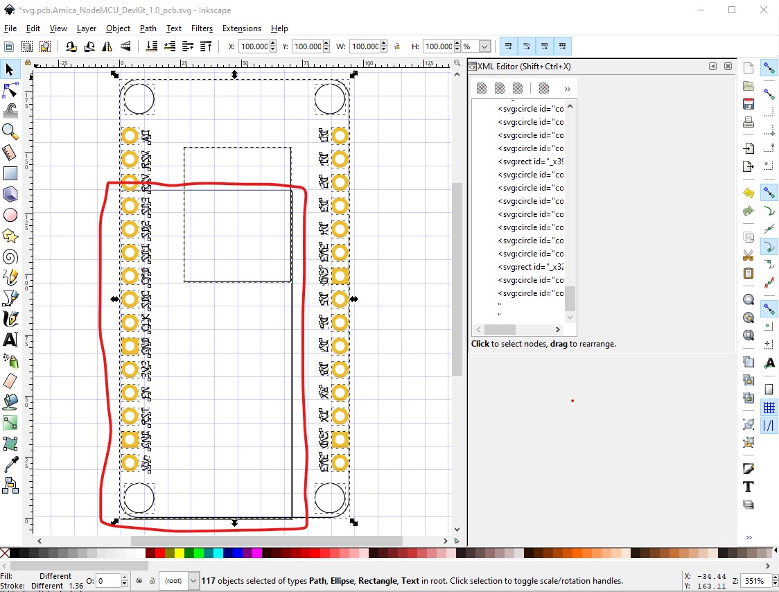
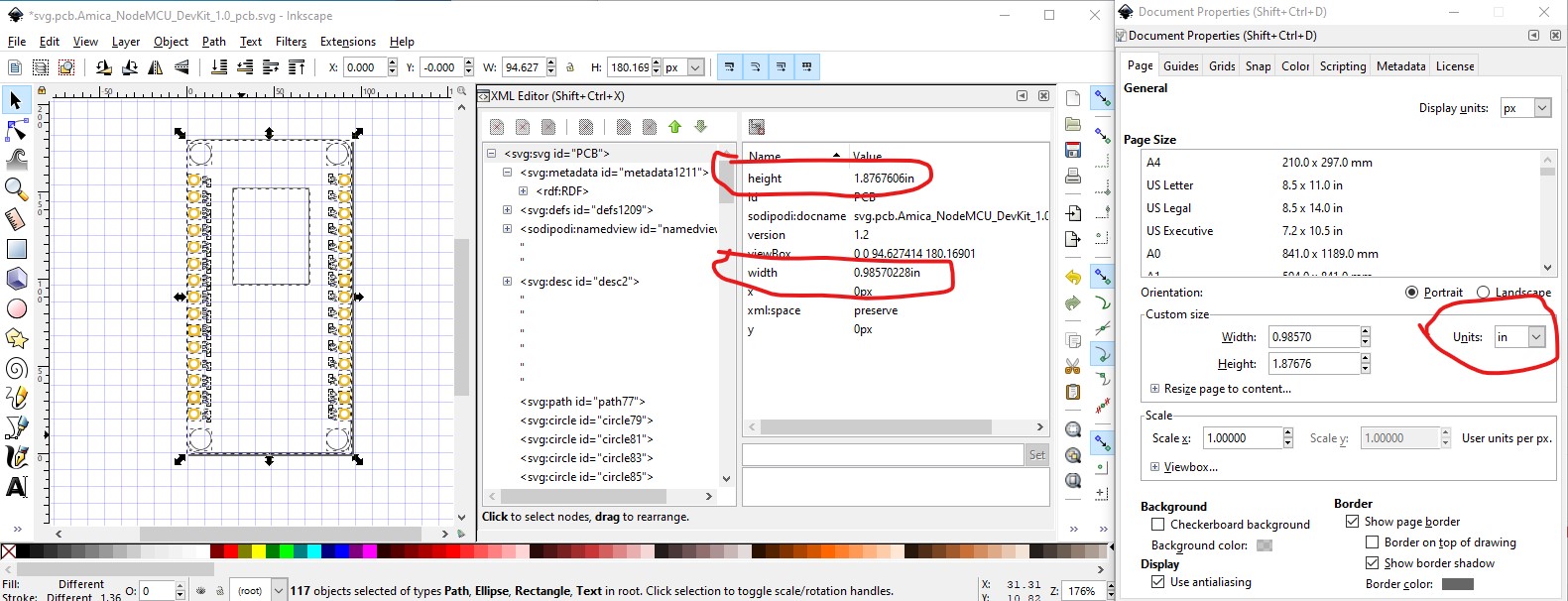
The original size of the board was the outline circled in red, the new size (as we see from the grid lines) has the pads in the correct places. Now we need to resize the drawing to reset the view box, and change the dimensions from px (editor dependent) to in (fixed) which has the effect of changing all the internal values and setting the height and width to in in the xml (circled in red here):

With a few more changes (scaled up to the standard scale and clean some things up a bit) this is the pcb svg in the new part. As before, I don`t know how to do this in Illustrator or if it is possible though. I changed all the pads to be standard .1 header pads, that is the hole is 0.038in and the ring thickness is 20 thousandths. This should produce a correct pcb for the original poster. Note that if you want the mounting holes drilled, you need to drag a hole from core parts pcb over the mounting hole in silkscreen in the sketch and adjust the size of the hole to match the mounting holes, by default the mounting holes are not drilled.

Amica NodeMCU DevKit 1.0-improved.fzpz (40.0 KB)

Peter

Thanks @vanepp, but I’m not sure we’re identifying the real problem here. The dimensions are all as we would expect inside Illustrator, where one works in inches or mm as one prefers (not in pixels), and there are clearly some problems importing Illustrator SVG files (which insist on presenting dimensions in Adobe’s idea of pixels) into Inkscape.

But in creating my parts, I use the Fritzong Parts Editor to do the initial compilation of relevant files. Now, the Parts Editor may be a bit flakey, but it does the original translation of the Illustrator SVG file and converts from pixels to inches. Unfortunately, the present example is not the best to be discussing here (we’d really need to go back to the original part), because I just modified the SVG file to increase the size of the pads, and didn’t then go back through the whole ‘construction’ process. As a result, the dimensioning inadvertently reverted to ‘Illustrator units’.

But the Fritzong Parts Editor, I would suggest, correctly translates Illustrator’s pixel dimensions into inches, using a scaling factor of 72. That translates the original 134.363px x 70.3px dimensions into 1.86614in x 0.976389in (although this conversion suggests that the scaling factor is just 72.00—i.e. correct to only two decimal places), as can be seen in the original part file.

Quite apart from everything else, in the Inkscape example you present, that translation does not appear to be symmetrical or as accurate—the scaling factor on the X-axis appears to be 71.59, while on the Y-axis it’s 71.32. I am guessing that this translation is automatic, but I would have to ask why the X-axis is being scaled differently, albeit only slightly, to the Y-axis? And looking at the PCB SVG in the ‘improved’ part, the scaling seems to be different again.

The scaling does seem to be the main problem here, at one level at least, but I’m not sure we’ve identified the source of this problem.

You are right, there is something else going on here. I just ran your original part through gerber processing and while the holes are too small (0.028in) and the spacing is a little off, but it is not as off as far as the picture of the boards:

From the gerber drill.txt file from the original part:

X021160Y017739
X012222Y017739

X .8938in (should be .9in)

X012222Y016743
X012222Y015748

y 0.0995in (should be 0.1)

X012222Y014752
X012222Y013756
X012222Y012760
X012222Y011765
X012222Y010769
X012222Y009773
X012222Y008777
X012222Y007782
X012222Y006786
X012222Y005790
X012222Y004795
X012222Y003799

So there is something else going on. @marcellodipietro how was the broken pcb made? Generated the gerber files and made by a board house, or printed and hand etched? The part looks mostly right, or at least not as wrong as the boards indicate.

Peter

I thought this post was going to appear above, with the posting of my modified part, commenting that it should not be used. In the event, it just appears down here, in sequence. Nonetheless, my apologies for trying to shortcut the process to generate this part. The following includes the bigger pin holes and uses the correct scaling:

Amica NodeMCU DevKit 1.0 (2).fzpz (56.3 KB)

As it is based on my existing artwork, it would be the basis for any further modifications I might make. If you don’t care about anything else I might do, then you’re probably just as well or better off using the version created by @vanepp, since he’s been playing this game much longer than I have and his part will be entirely consistent with Inkscape, rather than Illustrator.

Also, further to another comment I made above, I have no problem fitting female headers in 28mil holes, but I note that the male header pins are indeed larger and so require a larger hole (per these latter versions of the part).

This looks good! Did you find a way to change the dimensions from px to in in Illustrator or copy an svg already set to in? One small nit: in pcb group Pin_Holes isn’t needed. They are grey circles overlaying the pads although they currently don’t render in Inkscape (I’m not sure why because they should as far as I can see!) but will be ignored by Fritzing.

Peter

I can’t find anything in Illustrator to do the unit conversion, and based on my search efforts no one else has been able to either. But it does seem that all I really need to do is to manually calculate the converted dimensions (i.e. divide the pixel dimensions by 72) and simply change the “height” and “width” parameters at the head of the SVG file [in a text editor] to the resulting values (e.g. height=“134.363px” to height=“1.866153in”), although the ‘safest’ way to do things at the moment is to just use the Parts Editor. I’d be happy to do everything with an appropriate text editor (like I see you doing with Inkscape, but Inkscape, as I’ve mentioned, is just too much of a pain to use on a Mac), but there are still some things that the Parts Editor does for me that I don’t know how to do myself.

My current process involves:

  1. Preparation of the relevant artwork in Illustrator;
  2. Saving, in SVG format, the individual ‘subsets’ of this artwork that comprise the breadboard, pcb and schematic elements of the Fritzing part—the pcb artwork is invariably based on the breadboard artwork, with appropriate changes to colours, and sizes if this is required to create the right sized pcb elements (per the above discussion). At this point, all of these files are dimensioned in pixels, as is Adobe’s want
  3. Creating a new part in the Fritzing Parts Editor, at this stage using a closely related part from the existing library as the initial base. I would actually be happy to start from scratch, but this does not seem to be an option at the moment;
  4. Replacing each of the views with the artwork for my part;
  5. Updating the relevant metadata and connector details;
  6. Linking individual pins in individual views to the respective connectors;
  7. Saving the new part with an appropriate name, then exporting the part file. At this point, the essential ‘pixel’ units have been automatically converted to inches by the Parts Editor, some additional ‘Fritzing’ header information has been added to the SVG files and the little boxes that are the connection points in the Schematic view, have been inserted into that SVG file. The fzp file, containing all of the metadata and relationships between this and the individual views has been created and everything has been ‘zipped’ into the new part fzpz archive file.
  8. I then run the resulting fzpz file through your ‘parts washer’, which expands the archive;
  9. Next I change the names of all of these files, and their internal references, to those that are to be used in the final part (I’m not sure if the naming details are provided elsewhere, or whether I just worked them out along the way);
  10. I then run the FritzingCheckPart Python script over these files. If I’ve done everything ‘according to Hoyle’, I get a [more or less] clean bill of health. If not, it’s a case of ‘Wash, Rinse, Repeat’, going back to the relevant point required to fix whatever problem is exposed. There are several warnings that I regularly get at this stage that would appear to be the result of my using Illustrator way back at the beginning, but none of these appear to be critical.

And those ‘Pin Holes’ should never have been there. I think they will just have been an artifact carried over from the origiinal artwork and because they were never rendered I just didn’t notice that they were still there. This was the first part I made, so my process wasn’t as refined back then.

In addressing the current issue (increasing the pad/hole sizes) I have also discovered a problem with the way Illustrator deals with unit conversion. No matter what units I use, I find that I can enter exactly the same number in two different locations—e.g. x and y values—but occasionally end up with two different numbers if I change the units (through the Illustrator Preferences—only in the third or fourth decimal place, but occasionally they’re different).

As a result, there’s now a step ‘9a’ in the above sequence, where I check the PCB SVG file to ensure that the radius of all of the holes that are supposed to be the same, are indeed the same. The error is only ever in the third or fourth decimal place, so it probably doesn’t matter, but it can produce a ‘messy’ Gerber drill file—two or three different hole sizes for what should be the same size holes, although the fabrication process may not ultimately differentiate between them.

Yes this is a consequence of using floating point. The round offs cause small errors. One of the things I hope to make FritzingCheckPart do eventually is round off all the numbers (or at least most of them) to 2 or 3 digits after the decimal which should cure this problem, but I’m not there yet.

Peter

See how you go with this one (pads 1.447mm/0.058in).
Amica_NodeMCU_DevKit_1.0 (v2).fzpz (56.8 KB)

This one works and the NodeMCU amica fit without problems

Rather than start a new post, I thought I’d keep everything in one place and add these parts for recently released updates to the Heltec Dev Boards here.

The CubeCell V2 update is pin-compatible with the original, but I’ve also updated the PCB and Schematic elements of the original part, so they’re both included. The only real difference between the two is some minor changes to the Breadboard view to reflect the presentation of the updated module.

HeltecCubeCellDevBoard

Heltec CubeCell Dev-Board.fzpz (54.0 KB)

EDITED: Please note, this part file has been corrected in line the recommendations offered below in this thread.

HeltecCubeCellDevBoardV2

Heltec CubeCell Dev-Board V2.fzpz (62.2 KB)

The WiFi LoRa 32 V3 and Wireless Stick Lite V3 parts are based on a new ESP32-S3 processor so, while they each share the same form factor as their respective predecessors, they are not pin compatible with earlier (V1 & V2) versions.

HeltecWiFiLoRa32V3

Heltec WiFi LoRa 32 V3.fzpz (58.4 KB)

Heltec Wireless Stick Lite V3.fzpz (59.7 KB)

1 Like

I ran FritzingCheckPart.py against the files which detects the following error:

$ FritzingCheckPartw.py part.Heltec_CubeCell_Dev-Board.fzp

Error 69: File
‘svg.breadboard.Heltec_CubeCell_Dev-Board_breadboard.svg.bak’
At line 25

Found a drawing element before a layerId (or no layerId)

This will cause the part to not export as an image (svg, jpg, png etc.) to fix it, do an Edit->select all then Object->group (assuming Inkscape!) then name the resulting group “breadboard”

$ FritzingCheckPartw.py part.Heltec_CubeCell_Dev-Board_V2.fzp

only warnings which don’t affect functionality so fine as is.

$ FritzingCheckPartw.py part.Heltec_WiFi_LoRa_32_V3.fzp

Again only warnings which don’t affect functionality so fine as is.

FritzingCheckPartw.py ‘part.Heltec_Wireless_Stick_Lite_V3.fzp’

Again only warnings which don’t affect functionality so fine as is.

Peter

My first reaction was “Gee, I ran FritzingCheckPart on that and it didn’t report any errors…”. Then I looked again at the output and, sure enough, it did! But the strange part is that I didn’t change anything in the breadboard file, so that problem’s been there all along.

Fixing it was slightly more complicated because I use Illustrator, but all should be OK now.
EDITED: Following the recommendation offered by @microMerlin below, I have amended the file available through the link above.

As a matter of interest though, when we rectify a problem like this, are we able to automatically link the new file to the old posting, or disable the old link, or have it point to the updated post automatically?

Thanks.

If you have enough privilege, you can just edit the original post with the bad uploaded part. Delete that link from the post, and upload the new one. Optionally with an “EDITED” note to explain what you did.

Thanks @microMerlin, I believe that I have modified the relevant link and included appropriate comments in the above posts.

Yep, the new file appears fine so all should be well.

Peter