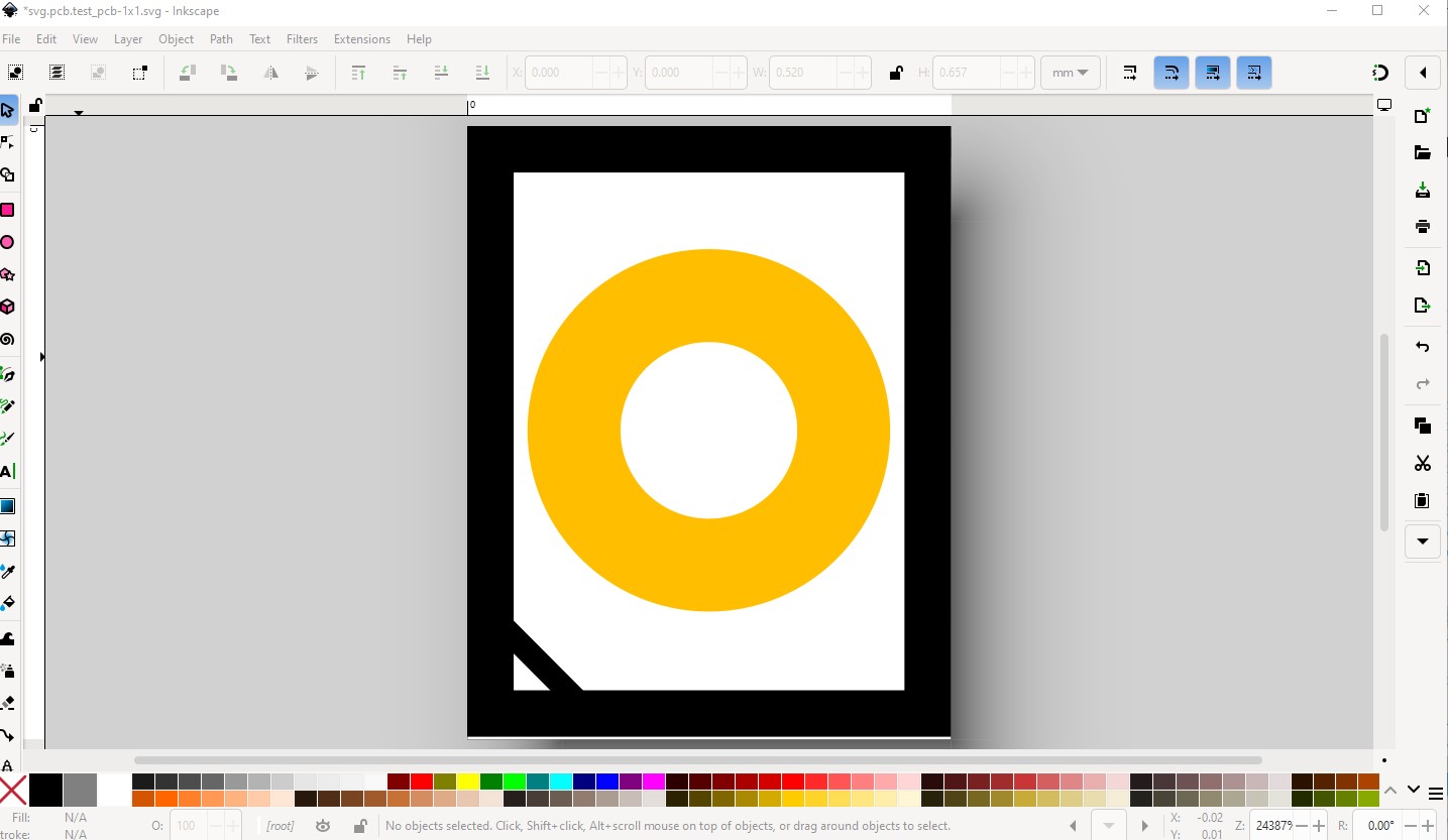
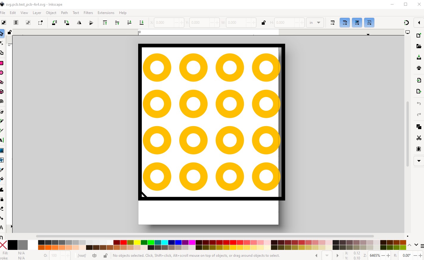
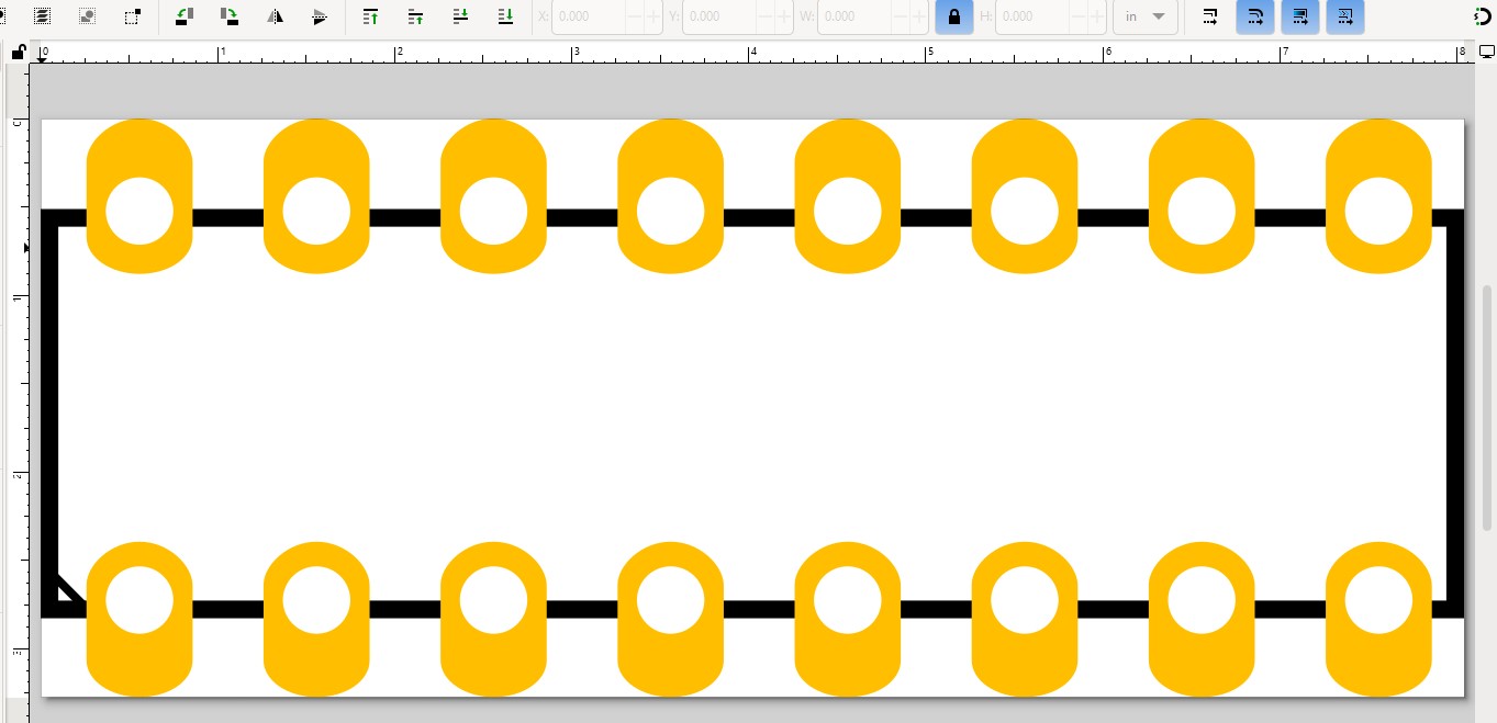
I am working on (and have been for a couple of years now) a python based potential replacement for the parts factory. Much of it is working fine, it can create (and scale to arbitrary pitch) headers both male and female, change their color and create unlimited rows and columns (although that is of limited use beyond about 4x4 because you can’t route traces to the interior pads!) For the last year or so I have been beating my head against the wall on setting the height, width and viewbox of the svg. For breadboard and schematic views it works fine (but they both have no elements with stroke-widths in them which I suspect is my problem.) The pcb view has a rectangle in silkscreen (and circular pads which may also be an issue.) The current parts factory I think just emits lines not rectangles, but I think does have stroke widths, but it works correctly. The viewbox they calculate is slightly large but it works. For me it doesn’t and I can’t figure out why. Here are an example set of svgs for a 1x1 male header and a 4x4 male header. The 1x1 header works fine (as it should as it was the test case to set the height and width values.) However as noted the 4x4 case works in schematic and svg but fails in pcb like this
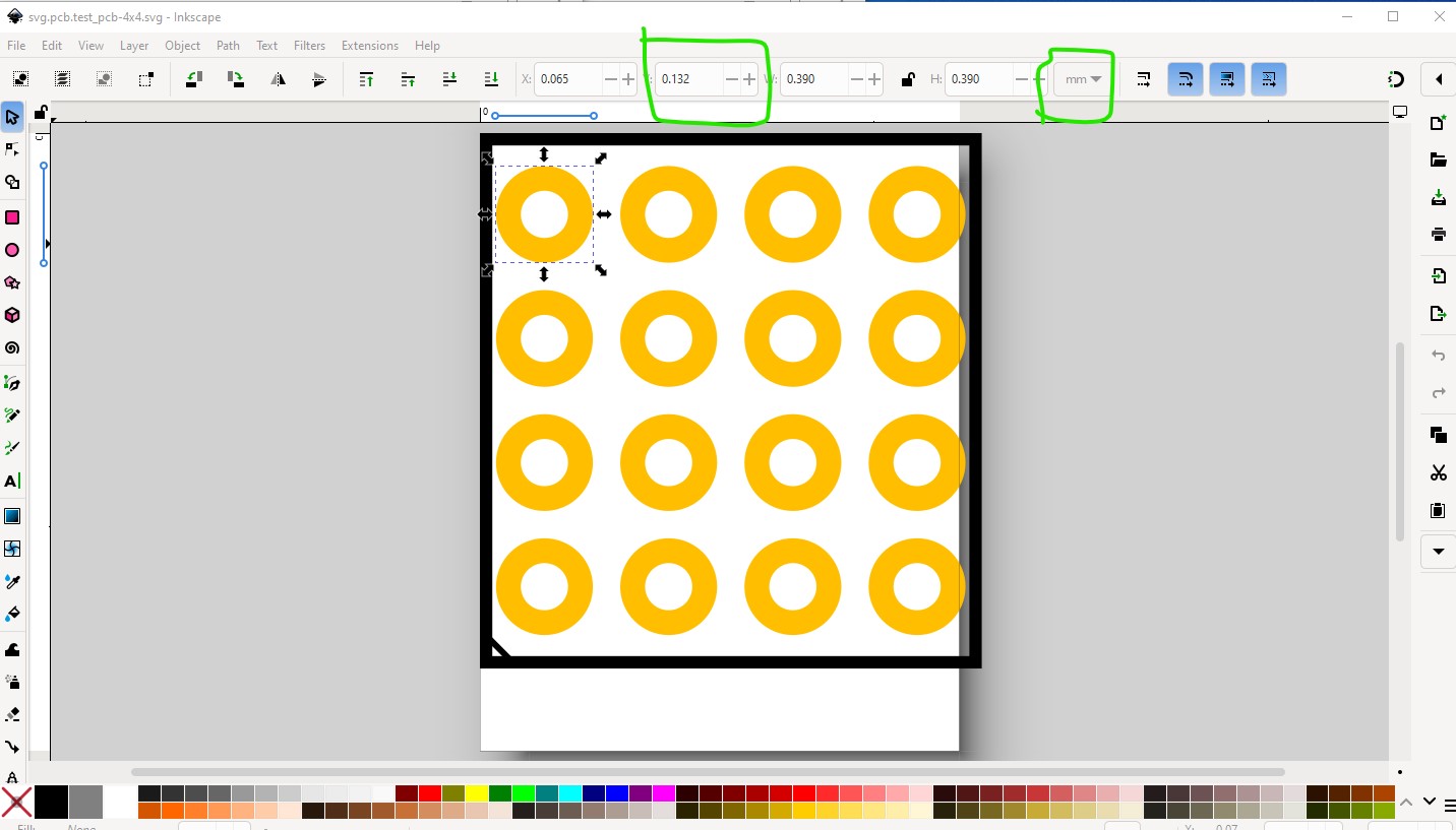
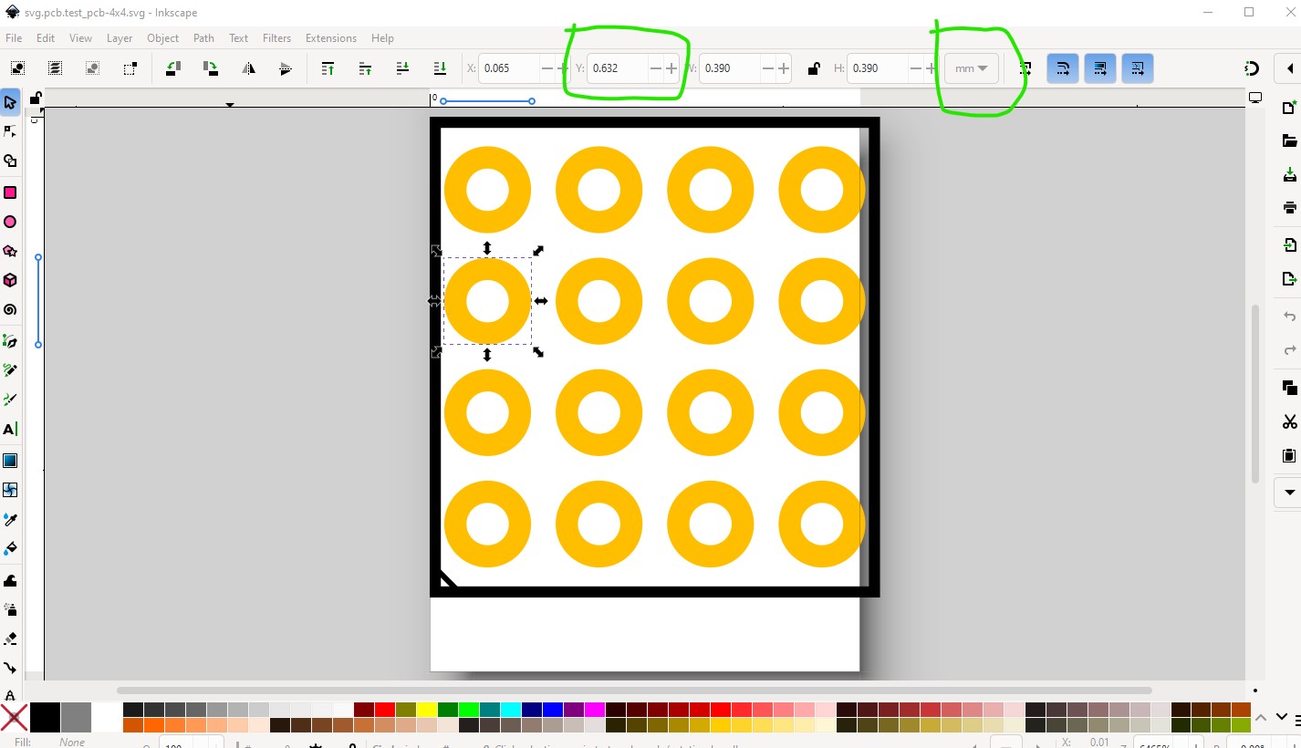
the not working 4x4 pcb svg also displayed in Inkscape. I would expect this to be wrong in the same direction, but it is wrong in opposite ways (too small in x and too large in y.)
the svg height and width are incorrect, although they are set to 4 x the values for 1 pin. The width is too short and the length is too long.
here are copies of all the svgs so you can look at the xml (since an error that I am not seeint in the xml is one possibility!) They are almost invisible here because they are 0.5mm pitch which is the smallest commercially sort of available header I could find. There are no data sheets I have been able to find and only one or two suppliers that list them (with large volume minimums!)
1x1 pxb svg
4x4 pcb svg
1x1 breadboard svg
4x4 breadboard svg (you can sort of see this one!)
schematic 1x1 svg (scaled to 0.1in so visible)
and the 4x4 schematic svg
can anyone see what I am doing wrong here? @KjellM or @microMerlin I think one of you are the most likely ones to have an answer, but I’ll take any suggestions anyone wants to offer!
Are those supposed to be 0.1in spacing? Your description does not say. I have not wrapped my head around where you are getting the numbers from. the 4x4 pcb has a spacing of apparently 19.685 mils. If I got the units right. It has been awhile since I looked at svg in that detail. I’ll find some of my reference templates that had .1in (100 mils) spacing. The svg header says the 4x4 pcb is only 0.09in in the longest dimension. That should be close 0.4in. From 3 x the spacing, plus the outside diameter of a circle, plus 2 times the silkscreen stroke width, plus 2 times the gap between silkscreen and outside of circle. I never use an id on the svg element itself.
Fritzing doesn’t demand the SVG to be in inches, you can use mm as well.
So, when you design a part that uses a 0.5mm pitch, instead of 1/1000inch units, you might want to use 1/100mm units.
That would make the numbers easier to handle, and mistakes easier to spot.
viewbox 0 0 250 250
width=2.5mm
height=2.5mm
For a 0.50mm pitch you could than have donuts at x = 50 100 150 200 .
And a square around a 4x4 could be d=“m10 10 h230 v230 h-230z” .
Due to the silkscreen and the pads themselves not being the same size as the spacing between them, the numbers do not work out quite that simple, but yes 1/100mm or 1/1000in are my ‘goto’ choices for units. Nice clean increments, but with some ‘fudge’ for an offset.
Sorry for the confusion, no they are not 0.1in pitch but 0.5mm pitch (the smallest non scaled header size.) although the svg is dimension in inches. If I change Inkscape dimensions to mm the spacing appears correct (although the internal units are in mils.)
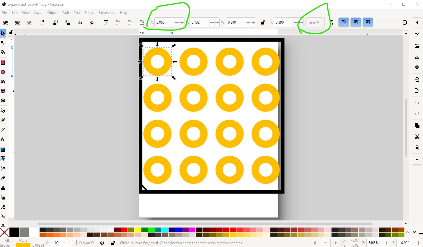
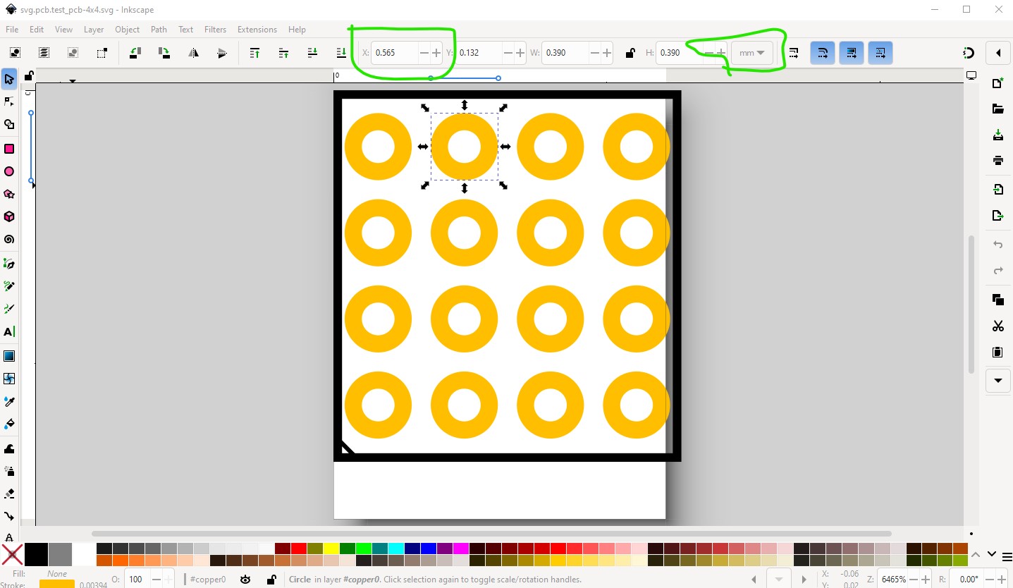
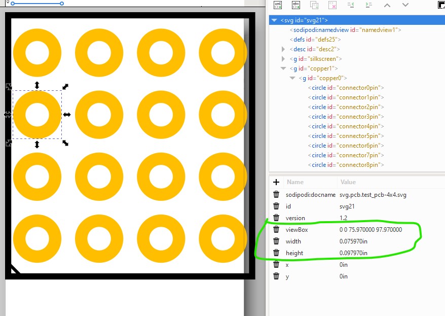
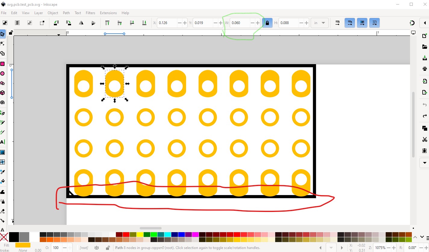
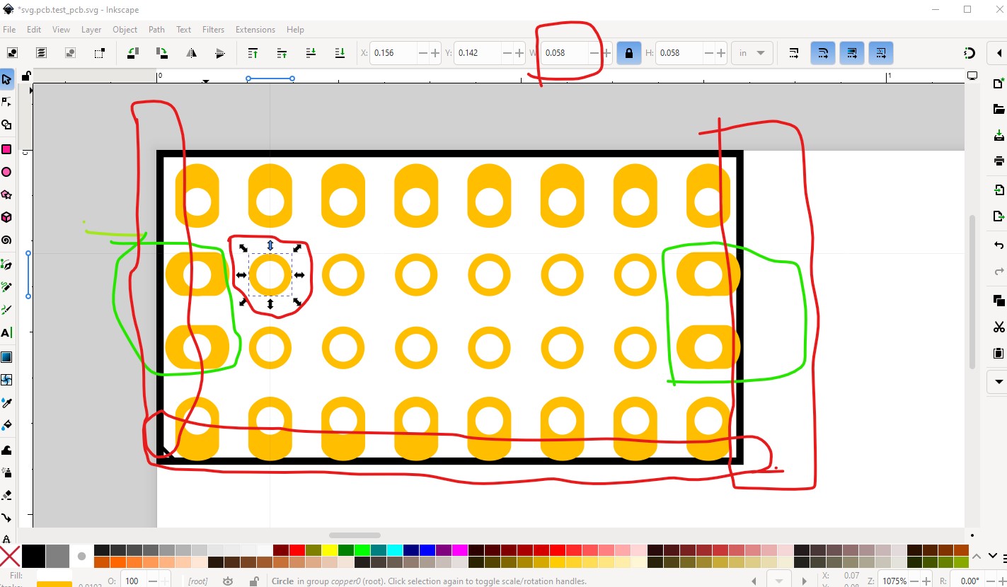
@KjellM It may be worth changing the viewbox and height calculations to mm as you suggest to see if that helps any. As you say it should make errors easier to spot. Although changing to 0.1in pitch should do the same (as the svg units will be in 1 mil units) so I should try that first I think. As far as I can see the rendered image is correct, it is only the viewbox I am having problems with. If I ungroup the svg then use Inskcape to resize the viewbox the viewbox changes to correct values, but the values it uses make no sense to me. They are non linear and I would expect them to be linear. I’ll try the suggestions above and see if I can figure out what is wrong. Here is why I think the rendered image is correct.
Set Inkscape to mm first pad starts in x at 0.065mm
Here I ungrouped everything, then did an Edit->select all and Edit->resize page to selection which corrects the view box but the numbers are very different (and don’t go up linearly with number of pad increases which I think they should.)
I’ll poke some more at things and try changing the sizes to mm for mm pitch elements and see if that tells me anything interesting. Thanks for the suggestions I at least have some further things to try while beating my head against the wall!
@vanepp You are aware that the silkscreen rectangle is not a square, right?
I am not sure how you derived this rectangle.
I’d expect it to be spaced evenly around the 16 connectors. So, maybe set try to set the width and height of the silkscreen rectangle to equal size, and center it around the connectors?
Yes, it is unsymmetrical for a reason. The silkscreen is intended to be the same with a circle as the pad (the case here) or an oblong (so that the trace can run between the pins) or a smaller circle (for middle pins in an array) so that traces can go any direction as required. The unsymmetrical silkscreen means the header is always the same size no matter which connector type is selected. I don’t think that should make a difference, but I have been wondering if it does as the breadboard version (which is symmetrical) works as expected. The objective is to allow this
Since the silkscreen isn’t supposed to be square, a viewbox of 79.53 by 84.92 (a bit higher than wide) seems to be correct.
In most cases, the viewbox would be the bounding rectangle for the outline of the silkscreen. It can be bigger tough, this would not directly be an error.
I see that, the parts factory headers are about 0.4in wider and higher than the actual silkscreen value. My problem is that when increasing the number of pins the viewbox doesn’t appear to scale linearly (possibly because I am doing something wrong) and gets worse when I scale the part from 0.5mm pitch to 0.1in pitch. The image above is an example, at a 1x1 single connector the viewbox is correct. At the 4x4 it is too short in x and to large in y even though it is specified as 4 x the 1 x values. I think your suggestion of changing drawing units to mm in the 0.5mm svg is a good next step, that should make the numbers much clearer in Inkscape and turn up any problems (or as always seems to be the case in this, cause more confusion!) There is code in there which scales the image (in the 0.5mm case the scale factor is 1 so it should be 1 to 1 and is why I am testing there.) At 0.1in pitch it multiplies by 5.08 (0.5mm to 0.1in) and for breadboard and schematic (which is always 0.1in pitch) that works correctly, but for pcb it doesn’t.
I don’t think 1x and 4x size is correct. For 1x, the silkscreen ‘extent’ should be the radius of circle (at least for horizontal direction) plus the circle stroke width, plus 2 times the gap between copper and the silk screen, plus 2 times the silk screen stroke with. the corner of the rectangle needs to (x and y) half of the stroke width.
For more than one connector, that needs to be (number of connectors (in a direction) minus 1) times connector spacing. Then add all of the rest. Since (number of connectors minus one) equals zero for a single connector, the same logic can always be used.
That will not be ‘linear’ scaling. Starting from the base for zero, the extent should have fixed size increments of the pin spacing. That will not be a linear ‘scaling’ (IE 1x, 2x, 3x, …). It will be
I just realized this is more complex than I though. I can probably cure the current problem by extracting the height and width of the rectangle and adding the stroke-width (as that seems to create the same value as the resize page to selection function in Inkscape returns.) Then I though I haven’t yet done the IC and it will have oblong pads as well, but the rectangle will be inside the paths and the bounding box will have to enclose those. A google search for “python 3 calculate svg viewbox” turns up a variety of hits and a suggestion to use syspathtools to do the job, but I think it only deals with paths not arbitrary elements like lines and doesn’t seem to give me correct answers anyway (although it may work better on the IC case with paths!) I am coming to think I just don’t know enough to do this, and maybe should write this off. I’ll poke a bit more at syspathtools and see if I can make anything work with that.
edit:
It looks like svgpathtools will do the job. It doesn’t deal with stroke-widths so in the rectangle case you get a offset from 0 which you need to add to the height or width term (then set the origin to 0) to allow for the stroke width but otherwise appears to work for everything (including the IC case where the oblong paths are in place) I have tested so far. It also doesn’t in this configuration deal with translates, but at present I don’t have any translates and it can be made to deal with translates as well (and maybe should be to avoid problems later.) I’m going to integrate this in to the code and see how it goes, so I may be back with more questions later.
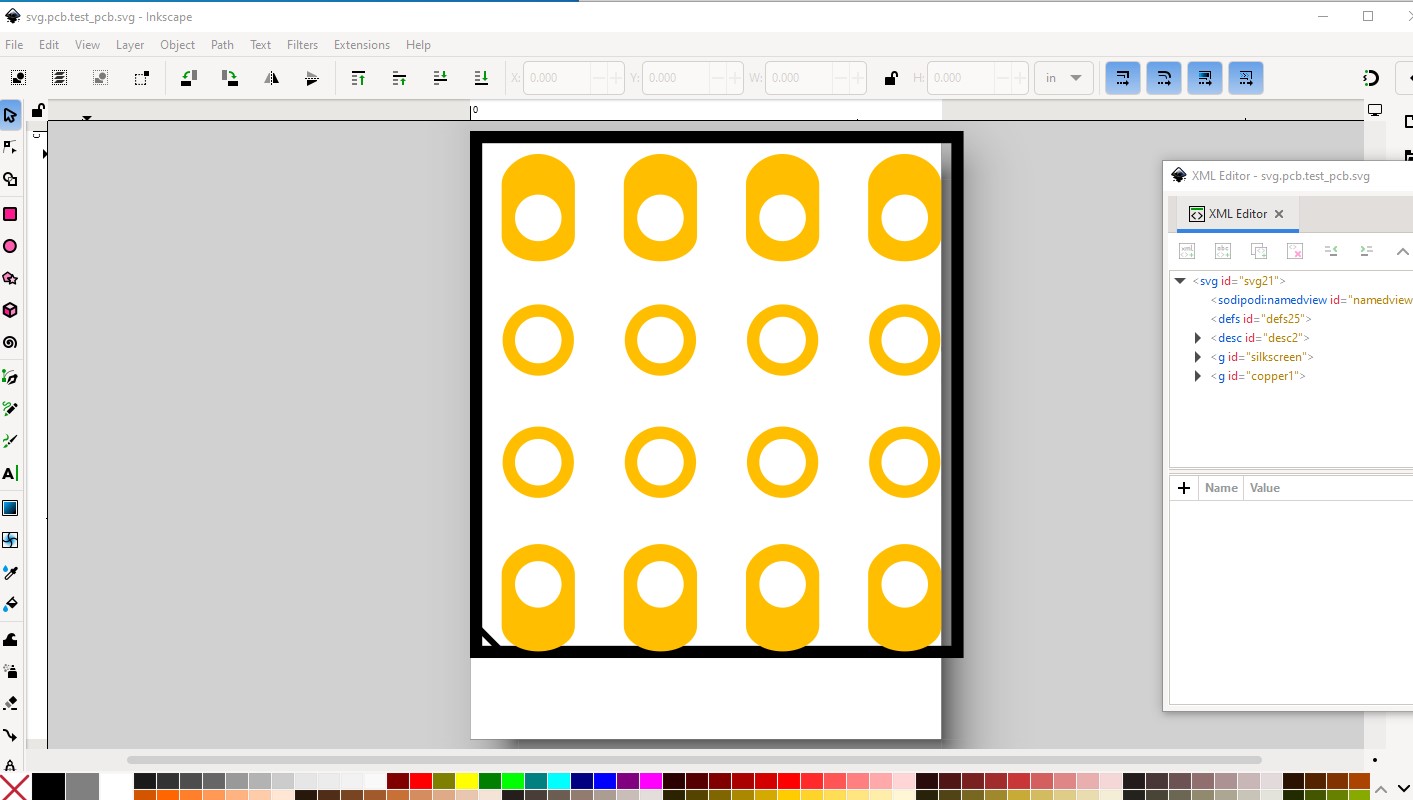
If the purpose of the oblong pads is to allow traces to connect to ‘interior’ pads, you might consider allowing oblong pads on all sides, pointing ‘way’ from the interior. An ‘edge’ case, but would be good for things like that 4x4 layout.
If there is an outer silk screen rectangle, that will define the extents (height, width, viewbox) for the complete file. Simple calculations. Any ‘messy’ stuff like the oblong pads will be inside of that, and not affect the extent. As long as only relative coordinates are used in those paths, they can be done once, then replicated with different starting points. They will not affect the viewbox at all.
When you do oblong pads, is the narrow direction of the pad less than the size of the (not oblong) interior pads?
At present the inner pads are a tiny bit narrower than the pad. I will probably boost the interior pad to the same size as the path for maximum copper. As well the silkscreen needs some adjustment as well it seems to be expanding non symmetrically. and the end pads being oblong too seems a good idea so I’ll do that too. I think this config will be the maximum usable as you will otherwise run out of space to route pads (unless you are running lines of ground or VCC to use on jumpers) but the capability is easy and may be useful.
With oblong (possible) all around, the silkscreen width needs to increase, and change the offset to the first pad. That would make the 1x silkscreen square again, with identical x and y offsets to the pad. The silkscreen rectangle width and height for other cases should be ‘simple’ math. The 1x size plus (n-1) * spacing for both x and y. With n being the count of pads in x and y directions.
Yes I am just changing the 0.5mm reference files to match that and then I’ll see what happens. I think the svgpathtools which appears to calculate a height width and viewbox the same as Inkscape may still be a better bet. It will handle transforms (such as may occur in polygons as Inkscape uses transforms to resize them and won’t remove the transform on ungroup, and thus may occur in some of the parts.) Progress at long last . The reference files for oblong at least is wrong (probably the others to) so that may be the source of some of the oddnesses I am seeing because the code is populated from the reference files. We will see how it goes.