[Help] Review needed for GGreg20_V3 Geiger counter module

Hi everyone,

I’ve just finished creating a part for the GGreg20_V3 Ionizing radiation detector (Geiger counter) by IoT-devices. This is my first time creating a complex part with custom PCB and Breadboard views, and I’m sure there are some technical issues under the hood (SVG scaling, terminal points, or XML structure).

The module has 4 pins (BAT-, BAT+, GND, OUT). I’ve tried to follow the copper1 → copper0 hierarchy for the PCB view and used a black rectangle for the silk mask.

Could someone please run this through the FritzingCheckPart script and check if the connectors are properly aligned and the SVG code is clean?

Any feedback or “fixed” version of the file would be greatly appreciated! If possible, could you please provide a corrected .fzpz file with the necessary fixes, as I’m still learning the technical requirements?

Best Regrds,
Oleksii Yanko

co-founder
IoT-devices LLC
Kyiv, Ukraine

Name of the part❗
GGreg20_V3 - DIY Geiger counter module

Your previous work, similar parts
In case there are similar Fritzing parts, or you already started work, please link it here.

  • I’ve created part by my own. See below.

Top view❗

The part file to check:
IoT-devices GGreg20_V3 Geiger counter.fzpz (39.4 KB)

Datasheet❗
The official documentation of the part manufacture is linked here:

As a new forum user, I am unable to add multiple images. I am also unable to add a link to the module description, but it almost exactly matches the Datasheet PDF. Therefore, please write to me and I will provide the necessary additional information.

Footprint
Does not apply to breakout boards.

Type
I did not read this
Breakout board, sub assembly, plug in module (A)
Antenna (AE)
Battery (BT)
Capacitor (C)
Diode (D)
Display (DS)
Fuse (F)
Hardware , mounting screws, etc. (H)
Jack, fixed part of a connector pair, header (J)
Relay (K)
Inductor, Coil, Ferrite bead (L)
Loudspeaker, Buzzer (LS)
Motor (M)
Microphone (MK)
Plug, moveable part of a connector pair (P)
Transistor (Q)
Resistor (R)
Thermistor (RT)
Varistor (RV)
Switch (S)
Transformer (T)
Integrated Circuit (IC)
Crystal, Oscillator (Y)
Zender diode (Z)
Other (please specifiy)
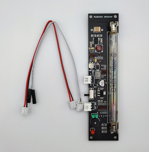
1 Like

The part already looks quite good.

The most important issue I think is

  1. missing layer ids for breadboard, schematic and icon. This will cause issues at least when exporting e.g. for print, but also confuses the automatic checks.

The breadboard svg should have a breadboard id, typically group <g id="breadboard"> .... </g> around everything.

Similar for the schematc, and less important, but lets be complete, also for the icon.

  1. The connectors in the schematic should be grey, not black.

  2. This is more personal preference, and depends how you want to use the board: In the PCB view, you usually don’t need detailed silkscreen drawings of all the elements. For a component like this, you often just want some connectors, where you stack it, or connect the cable. So, a minimal version of the PCB would just draw four THT connectors. If you plan to stack it, you could also mark the mounting holes for drilling, or add an outline of the board, so you see which space it will take up on your PCB.

There are some connector leftovers (incomplete) , like “connector11” , in the SVG.

I’ll try some cleanup since I am already on it.

I guess the bus is intended, it connects BAT_N and GND.

 <buses>
  <bus id="internal1">
   <nodeMember connectorId="connector8"/>
   <nodeMember connectorId="connector6"/>
  </bus>
 </buses>

Here is a cleaned up version. It should look and mostly behave the same, except for the export to SVG and similar options.

IoT-devices GGreg20_V3 Geiger counter_8.fzpz (36.2 KB)

If you like, the eagle2fritzing repository has a subparts folder with some graphics, that you could use to improve the breadboard illustration.

Edit:
For the illustration, it doesn’t matter that much, but the THT connectors look quite small.

The copper rings in the breadboard are 1.16mm diameter (2 * r=0.90 + ring=0.26 => 1.16) . The issue is that the stroke centers on the radius, so for a 0.9mm drill and 0.3mm ring, you would use r=0.6 , stroke=0.3 , adding half the stroke to the drill radius.

But a ring thickness of 0.3 (or even 0.26) still looks quite small.

1 Like

Thank you very much for your help. I will now download your corrected version of the file.
As I am a new user, I did not quite get your advice regarding the ring radiuses. I would appreciate some step-by-step instructions.
I understand that larger holes are better, but please could you give me more specific advice on what you think needs to be corrected.
Note: The connectors on the module were designed for pins and/or JST connectors with a pitch of 2.54 mm. Of course, in my source file for the electronic and printed circuit board, these holes have a slightly different and more complex geometry than the one I made for the connection points for the model in Fritzing, because I simplified it.

Thank you again,
Sincerely,
Oleksii

When I created the component in Fritzing, I added this internal connection because these ports are essentially a single line (BAT_N and GND). I did this using the Fritzing editor. I hope I did it correctly.