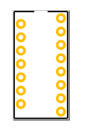
Hi, right now I’m creating the l298n chip for fritzing and I´ve already made the schematic and breadboard view, but when I´m creating the pcb view on Inkscape and putting the silkscreen part on the silkscreen layer and the copper holes in the copper layer and save them as an .svg, when i load the image to fritzing it just imports the copper holes, can someone help me with this problem?
The best bet is to upload (upload is 7th icon from the left in the reply menu) either the pcb svg (which sometimes doesn’t work) or the fzpz file of your part (which contains the svg) and I will have a look at it. The layerId on silkscreen (which is usually silkscreen) needs to match the layerId specified in the fzp file for the part.
Peter