It is not true that you have to have a double sided board. With a single sided board the copper is all on one side (the bottom by convention), but the holes go through and the parts mount on the other side. The holes would not be plated (I believe), but they still solder just fine.
Efficient can mean different things. You know the physical constraints based on where you intend to use the board. If you DO use a double sided board, moving some of the traces to the second side simplify some of the layout.
If you are going to include part labels as silkscreen on the pcb, they need to actually be positioned on the board, and located somewhere near the parts they are associated with. If some (or all) of the labels are not needed/wanted, turn them off. Right click a part, and choose “Hide Part Label” from the context menu. I did that for the Digispark board here, since the part has the name in its own silkscreen. I moved the rest of the labels somewhere reasonable. The labels could also be changed using Inspector. “Part1” may not mean much when looking at the pcb. That could be changed to “Bridge”, or something else. I changed “IC1” to “OPTO” as an example.
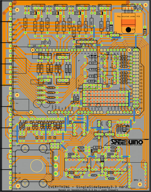
I assume that the physical length of the pcb is matched to the coach. pcb production is normally charged by board area, so if it does not need to be the full length of the coach, trimming the blank area from the ends will save some money.
You can add your own text in addition to changing the existing labels. You are controlling 4 individual circuits (lights?) in this version. You can add a text label to show what they are. I added “Ceiling” between J7 and J11 as an example. This view contains the adjustments described above (except changing board size).
Using a single pin header to leave a solder connection for the off board capacitor works. Another option would be to use a “Hole” part, and set the desired hole diameter and ring thickness. In this case, there is plenty of room on the pcb, so you could just include an electrolytic capacitor in the circuit, but know that it will be wired off board. That would include the capacitor silkscreen, and the holes would be the standard (narrower) 0.1in spacing.
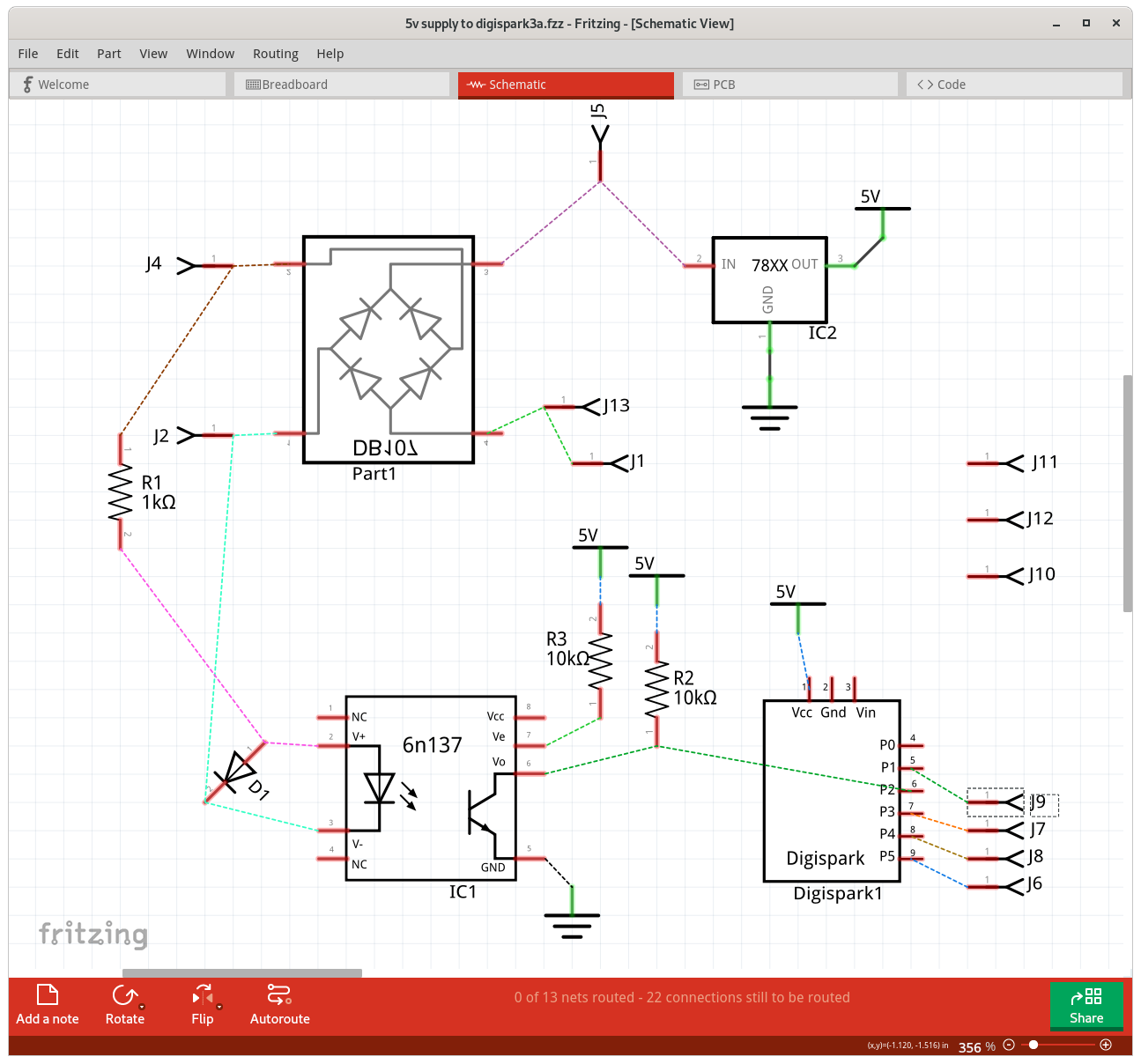
You should probably start (a project) by laying out the schematic view reasonably. If you do the wiring there first, the ratsnest wires (dashed lines) will show you where connections (traces) are needed on the pcb view. Here is an example of a rough layout for the way your circuit is currently wired, according to the traces you created on the pcb view. This was created by moving the parts and labels around. The only actual change I made, was to add the ground and 5V parts, and explicitly connect the voltage regulator to the 5V and ground symbols (the solid lines). Looking that over, you should see that currently some connections are missing. The digispark board gnd pin is not connected to anything. J10, J11, J12 are not connecting to anything either. J1 and J13 show as connecting to pin 4 of the opto isolator, but are not connecting to the ground for the rest of the circuit.
These things visually look fine on the pcb view. The reason they do no match the revised schematic view is that you laid down traces over top of each other, without actually telling Fritzing that they were connected together. The pcb view has a design rules check option on the routing menu. That tool is intended to help find places where traces and parts are too close to each other, or to the edge of the board. Running it on your existing layout complains a lot. Some of that is because it sees those overlapping traces, and thinks they are a problem. They are not “connected”, but the overlap.
DRC also complains that the pins on the digispark board should have copper on both the top and bottom of the board, but the svg for it only has a single copper layer. The part was not created following all of the rules that Fritzing uses. Someone here should be able to fix that easily.
DRC complains that the digispark part is overlapping the bottom layer. This because the trace you used for the gnd pin is not actually connected to the pin. It did not end on top of the connector. Which is why the schematic view shows no connection there either. That is the same problem for J10, J11, J12. The schematic shows them as not connected, and DRC says they overlap the bottom layer.
As I said above “efficient” can have different meanings. Here is one alternate that feels cleaner to me, but do not consider is as optimal, or best, or anything like that. As a general theme, I reduced the amount of board space needed for the active part of the circuit. In general, short leads are preferred, as are shallower bends in wires. Here, shorter leads would only matter if you could reduced the board size. In other cases it might be more important, and I almost always “practice” for the possible cases. This also leaves more room, if in the future you want to add to the circuit. If it works where you plan to place it, this version of the board could be narrowed somewhat. If double sided boards cost more, even narrower it could be more expensive. While I tweaked part and header positions, I did not adjust the board size. I used both sides of the board here. This shows an alternative to running the traces over top of each other. Run the trace to the nearest connection, then start a trace from there to next location. The obvious one for that is what I did for the ground pin on the Digispark. I did not fix the Digispark part, so all the connections to it still needed to be on the bottom layer, and DRC still complains about the single copper layer. But that is all it complains about now. I replaced the header pins with the capacitor, but there is no requirement to put it on the board. The wires off board you were planning are fine. In fact, I overlapped the silkscreen, so it would not even fit there.
5v supply to digispark3a.fzz (58.9 KB)
The schematic would be a little cleaner, if the part definitions had followed the Fritzing recommendations more closely. The pins for connections are supposed to be setup on a 0.1 inch grid. And should have “terminal” markers to show where connections will attach to the pins. The bridge rectifier is a little off, the Digispark a bit more. I did some clean up the breadboard view as well, but was not as fussy as elsewhere
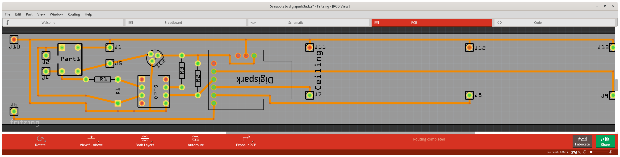

 -, but in the PCB you used the short cut of putting traces on traces. You can see J13 is ok and green, but if you click on J11 nothing else lights up yellow, ie, no connection. To add a bendpoint so a trace can connect properly right-click on the original trace and select create bendpoint. Or just grab the original trace and move it and put it back, and link from pin to BP. You can also ALT-click a BP and drag a trace to the pin.