Hello! I’ve never used Fritzing before, but I need some custom PCBs for a project. I’m hoping to learn the ropes with a relatively simple component - a breakout board for a chip I want to analyse (in fact, a 6502 CPU I pulled out of an old Commodore machine).
The problem is, I’m struggling to understand what exactly is meant by “top” and “bottom” in the PCB view.
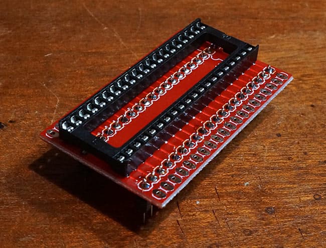
I basically want to design something like this “chip riser”, but for a 40-pin IC.
I can only attach one image as a new user, but there are two rows of male headers on the underside of the PCB, in the same pattern as the chip socket but offset to the right.
So, on to my confusion.
Assuming what we see in the picture is the “top” of the PCB, that should mean the actual copper is on the bottom, since you pass the pins of the chip through the holes in the PCB and solder them on the other side.
Similarly, if those male headers are on the “bottom”, then the copper (and solder) should be on the top.
Basically I wanted to confirm whether “top” means “the component is on the top” or “the copper is on the top”?
I also wanted to know what the best way is to just create a hole to solder a wire into, breakout-board style. You can see on both edges of the chip riser above, there are holes for this purpose - to solder wires directly into.
I notice there is a PCB “hole” component, but this seems to be for something like a screw hole, whereas what I really want is just the same sized hole as the ones for the male headers (which is what I’ll do if there isn’t a better way!)
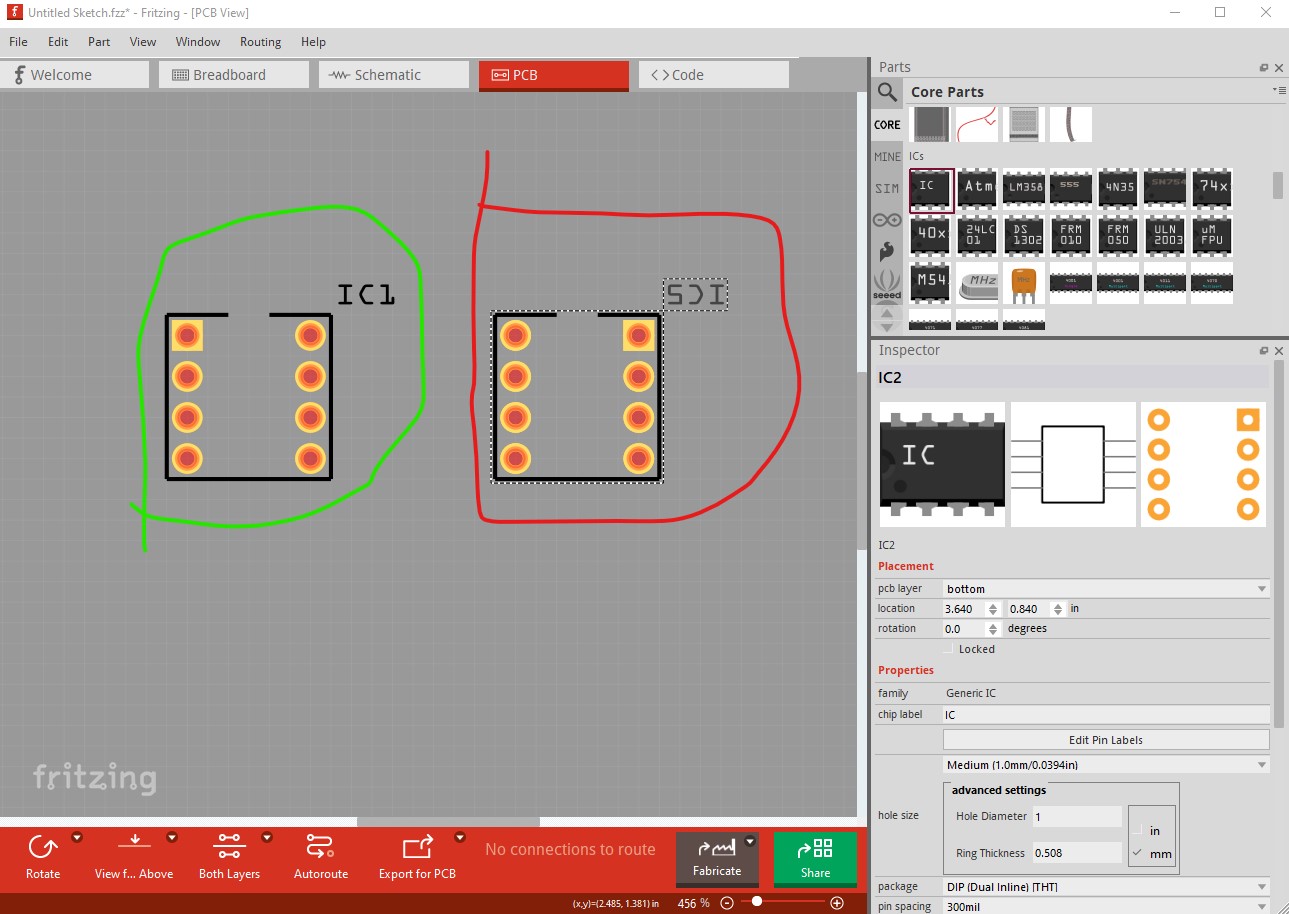
The top means the component is on the top of the board (the default.) If you select bottom it will flip the component to mount from the bottom of the board (so your socket will be on the bottom of the board and soldered on the top layer.) The pins get inverted (as they will be in real life) when you do this like this
the generic IC on the left is the default top of board. The IC on the right has been changed to bottom and expects to be mounted on the bototm of the board and soldered on the top. Thus its pins are inverted in x (and its label is on the bottom silkscreen layer.)
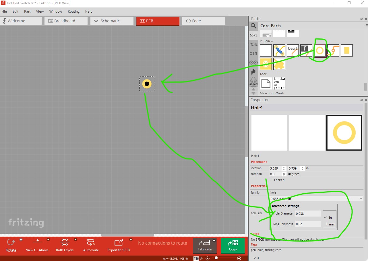
I usually use a single pin header. That gives you connections in all 3 views (which is usually what I want.) The hole will work the same, except it will only exist in pcb view not schematic or breadboard. As long as that is what you want it will work. The trick is to set the ring diameter which adds the ring (by default it is 0 and thus a hole) in Inspector like this
this sets the same pad a single pin header (0.038in hole, 0.02in ring) only in pcb (nothing in schematic or breadboard.) You can change the sizes as you need to. Hope this helps.