Getting a layout template into PCB

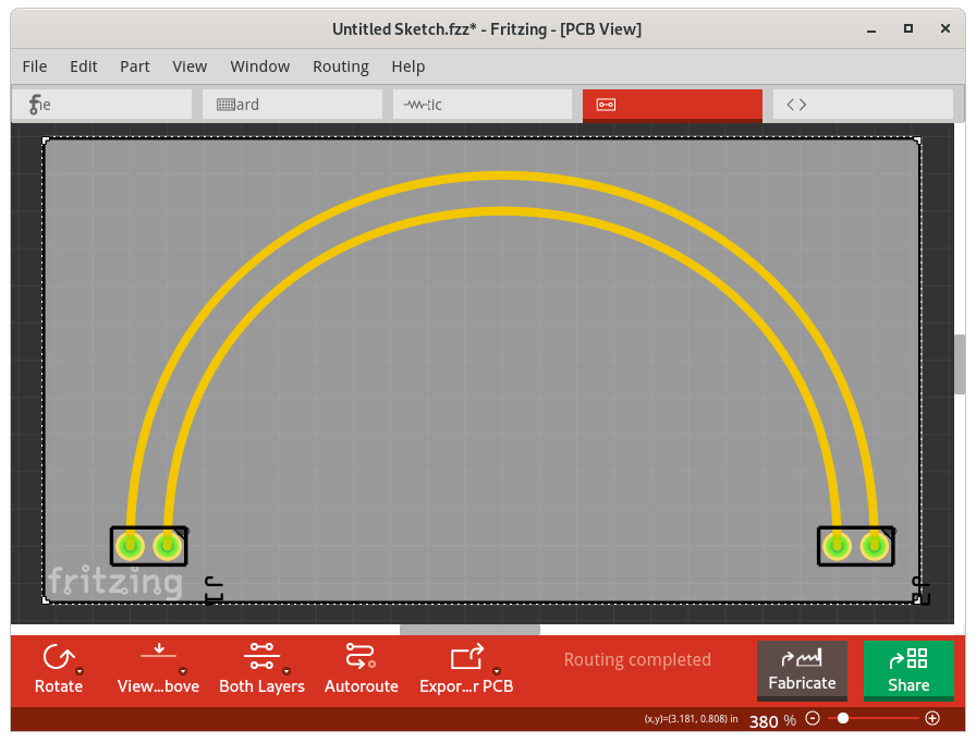
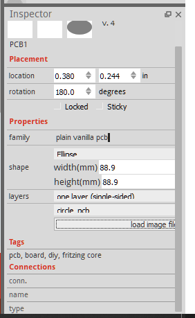
I am trying to make my first PCB board in Fritzing. The board color is solid almost-black, making it hard to figure out where my parts are. The outlines of the devices are black on a very, very dark background. I would like to change the part colors to white or the board color to something like light-green. This example was my first simple layout for 4 LEDs; the final one has 24 LEDs, and to get the placement correct I have a drawing (both in SVG and PNG) that I want to place on top of the board so I can rotate the LEDs in 15 degree angles. I can’t figure out how to insert the drawing as if it were a silkscreen layer (it will be removed before sending the board out for production). This board was originally rectangular, and I now have to rearrange everything for the new circular geometry. It would be nice if I could do circular traces with a radius, and I can’t discover how to do that either. Note that the LEDs are common anode, and I used one of the calculators on the Web to get the width of the traces for the load that the full 24-node unit will have.

Here is a screenshot of the PCB layout (old rectangular layout on top of new circular board)


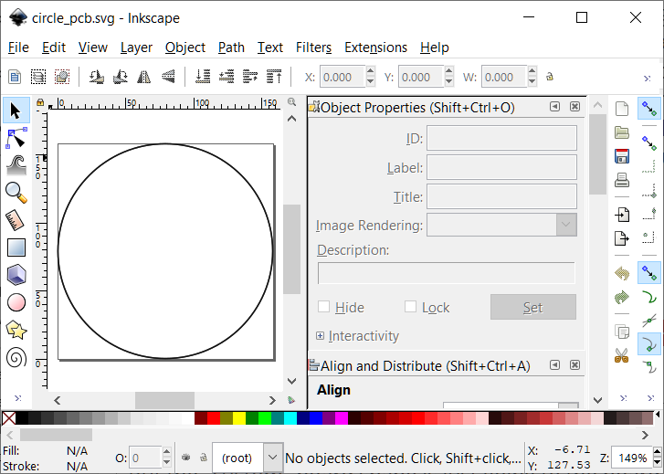
and here is the InkScape-generated PNG file that will help me get all the parts placed properly. The outer circle is the board, the inner circle is the outside leg of the RGB LEDs, and the angles are 15 degrees.
15 degrees
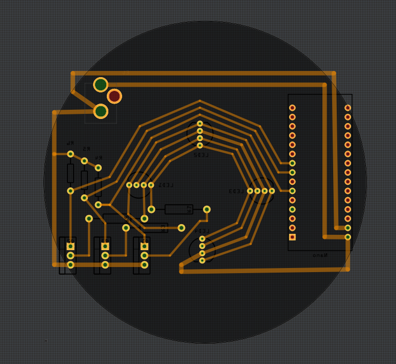
I was able to do this as a single-sided board, so what you are seeing here is the board view from the bottom. Because I will have to move the controlling Arduino Nano to the interior, I will probably end up with a double-sided board.

When creating a custom board shape, the board color can be set to anything you want.

I believe (this needs to be tested and confirmed) that one custom board can be replaced by another, and if they are the same size and shape, it will not affect the already laid out and routed pcb. So:

  • Create the circular board svg image with whatever color you want to use to do the layout
  • Include in that a silkscreen layer with the 15 degree lines and circle for the RGB LED legs
  • Copy that svg file to a new name, change the color to what you want to send to the production house, change to the final board silkscreen

Set the Frizting PCB view board to the first image, place, layout, route the parts and traces, then change the board image to the second file.

There is no way to directly create circular arc traces, but it IS possible to create curved traces. When routing wires or traces, clicking and dragging will either create a new bend point, or drag out a curve for the current segment. That is controlled in preferences (Edit menu, preferences) on a per view basis. However that is set, the opposite effect can be achieved by holding down the control key while click/dragging. The curvature can be controlled similar to some drawing tools. A pair of control points is generated interally to ‘pull’ the curve into different shapes. Dragging adjusts the control point for the end of the segment closest to the initial click point. While dragging, a construction line is shown for the direction and strength of the pull at both ends. Effectively the control points. Adjust to get those lines perpendicular to where the diameter of the circle should be, with equal lengths. Keep adjusting the lengths until the center of the curve is half the distance between the end points away from straight line.

if you know where the arcs are supposed to run, markers could be added to the board silkscreen, to help with alignment (some concentric circles). Rulers and other temporary graphics can also help. Even the grid. To get close to accurate curves, you need to turn off ‘align to grid’ while adjusting the curves. Here is an example created with a couple of 2 terminal connectors placed so the outer terminals are 2 inches apart. To get the outer circular arc, the control points lines needed to be about 1.32in long. With that, I would have guessed square root of 2 times the radius, but that is bit off.


Creating semi-circle traces this way is relatively easy. Shorter segments are a bit trickier. The main hint, is to keep the lengths of those control lines the same, and their angles relative to the straight line between the ends the same. I think that the simplest case, is to point those lines directly away from the endpoints of the diameter of the full circle. Where the diameter is parallel to the straight segment (cord of the circle). I think that will keep the target length of the control points lines the same as they would be for the full semi-circle.

But the “custom” board shape is just going to the board menu in the inspector and choosing “ellipse”, and setting the dimensions identical. I didn’t think there is anything else I needed to do to get the board; what is weird is that the board is such a weird, dark color. So when I select the circular outline. although it is hard to see, it says the file is circle_pcb (implied .svg).
fritzing3
So I found the file and opened it in InkScape. It is a completely plain circle.


So I am now confused as to what you are referring to when you talk about setting the color on the board in the .svg file. There is no color set in the .svg file. So it should be white.

I had never used the built in ellipse shape, so was not aware there was a problem with it. The rest (that I just tested) seem to work fine.

That is not what I meant anyway. There is another option shown in inspector to “Load Image File”. Creating an svg file, and using that, provides a lot more control. Use something like this file for the ‘first’ file described in the previous post

test_circle_pcb
That is 3.5 inches (88.9mm) diameter, with silkscreen concentric circles at 0.1in increments, and radial lines every 15 degrees. Board color is set to “green” and 50% opacity (so grid shows through).

You can save that image locally, then either use it as is, or create your own based on it. As for other images to be used with Fritzing, it has some “special” group names to be used for layers. Because of the very fixed coordinates needed (and I am used to it), I created that file manually in a text editor, but Inkscape (and other svg editors) can be used, as long as the correct group ids are used.

Got it working. Now the question is, since the circles and rays are on the “silkscreen” layer, how do I create an actual silkscreen with part outlines and such for the manufacture? If I hide the current silkscreen layer, all that stuff is going to disappear.

That is why my initial reply said to create 2 copies of the image. One with the working color and silkscreen, the other with the production color and silkscreen. After finished layout and routing, use the “Load Image FIle” again to load the second version. The silkscreen “part outlines” should be part of each individual part, and will not be affected by swapping the board outline and silkscreen. Only silkscreen for the whole board (not individual parts) needs to be part of board shape file. Things like board version number, title, logo.

As mentioned in the initial reply, that needs to actually be TESTED. Take a copy of an early work in process version of the project, do the image swap, and verify that nothing broke.

There are some more options as well. There are 2 skilkscreen layers. One for the top (“silkscreen”), and one for the bottom (“silkscreen0”). You could move the radial lines and concentric circles to the bottom, and use the top as normal. Then, before generating the gerber files for the production house, remove the bottom silkscreen. Fritzing can turn layers on and off (see the “View” menu), which is handy during project creation. You could turn off the bottom silkscreen to see what the final version should look like, then turn it on to help do layout. Same, you could turn off the top silkscreen, to get it out of the way while using the bottom graphics to do layout. It is not enough to have the layer turned of while exporting. I believe that the export ignores the view layer settings.

Alternatively, without removing the bottom silkscreen before export, the project could be exported with the extra silkscreen layer included, then that layer removed from the generated gerber content. The silkscreen layers are each exported to their own file, so that is as simple as deleting a file. Once you have verified which file is the bottom silkscreen using one of the gerber viewers (like gerbv). You need to do that anyway, to make sure that the export is complete and correct. Some parts work correctly in the Fritzing views, but are broken in such a way that they do not export, and no error is reported.

THANK YOU! You have been a tremendous help!