I have an application where I need to deliver 5 amps RMS to a load using a Form C relay.
Is there a Fritzing library model for a typical Form C, DPDT relay, such as the CIT J152 series with PCB pins? With the PCB pins, which are small size rectangular in shape, I could solder this relay to a PCB
While there are some relays around (a google search of the form “fritzing part relay” should find them) there doesn’t appear to be one for the listed part. You would need to specify which contact layout you want though (there are 3 options for the part listed) and the pads will end up holes of the maximum diameter of the pin as Fritzing doesn’t do slots in parts.
This part should do what you want. Schematic may be wrong as which is NO and which is NC is not clear from their schematic.
edit: Got the NO/NC pins wrong and the data sheet doesn’t match the physical part (the pads are out in x) so I have replaced the original with a corrected (I hope!) version.
Good Morning Peter: The relay pins in pin footprint on the model that you sent me did not line up with the J152 relay.
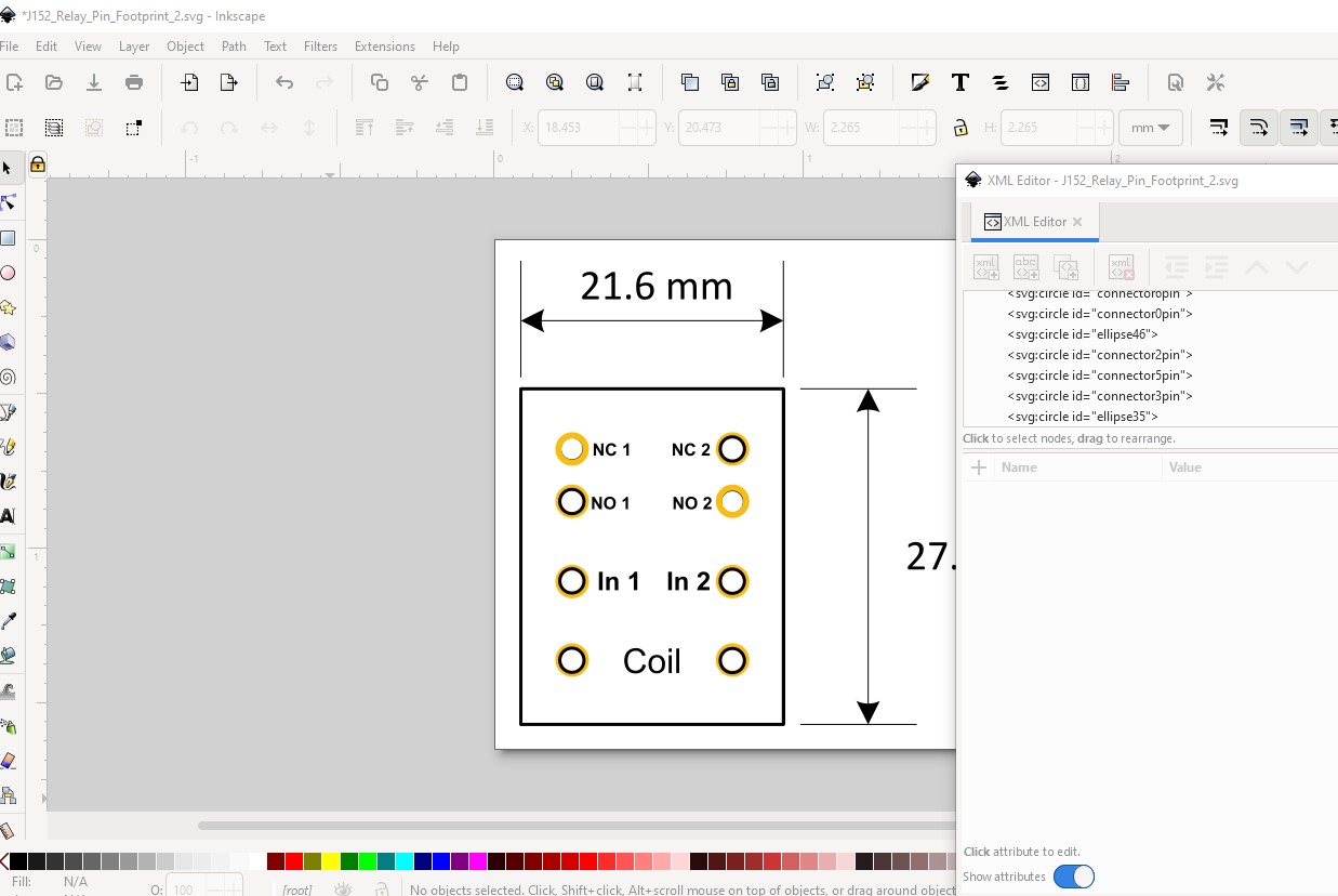
Using Visio, I created a pin footprint which does line up with the relay pins. The circles in this footprint are 2mm in diameter and seem to fit around the 1 mm x 0.5 mm relay pins rather well.
I also added pin labels as seen looking down from above the relay.
I saved this drawing as an svg file:
J152_Relay_Pin_Footprint.svg, which I send as an attachment to you.
J152_Relay_Pin_Footprint.svg
I hope that you receive this file. If not, please contact me and tell me how to send this .svg file to you.
I don’t think the forum does attachments (as there is nothing in the post!) The easiest is upload the svg directly (upload is 7th icon from the left in the reply menu.) That said the footprint should match the recommended one in the data sheet and the holes should be the requested size (1.3 or 1.5mm as I recall.) However it is easy enough to change it to the set in your svg.
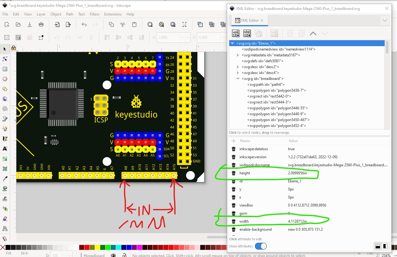
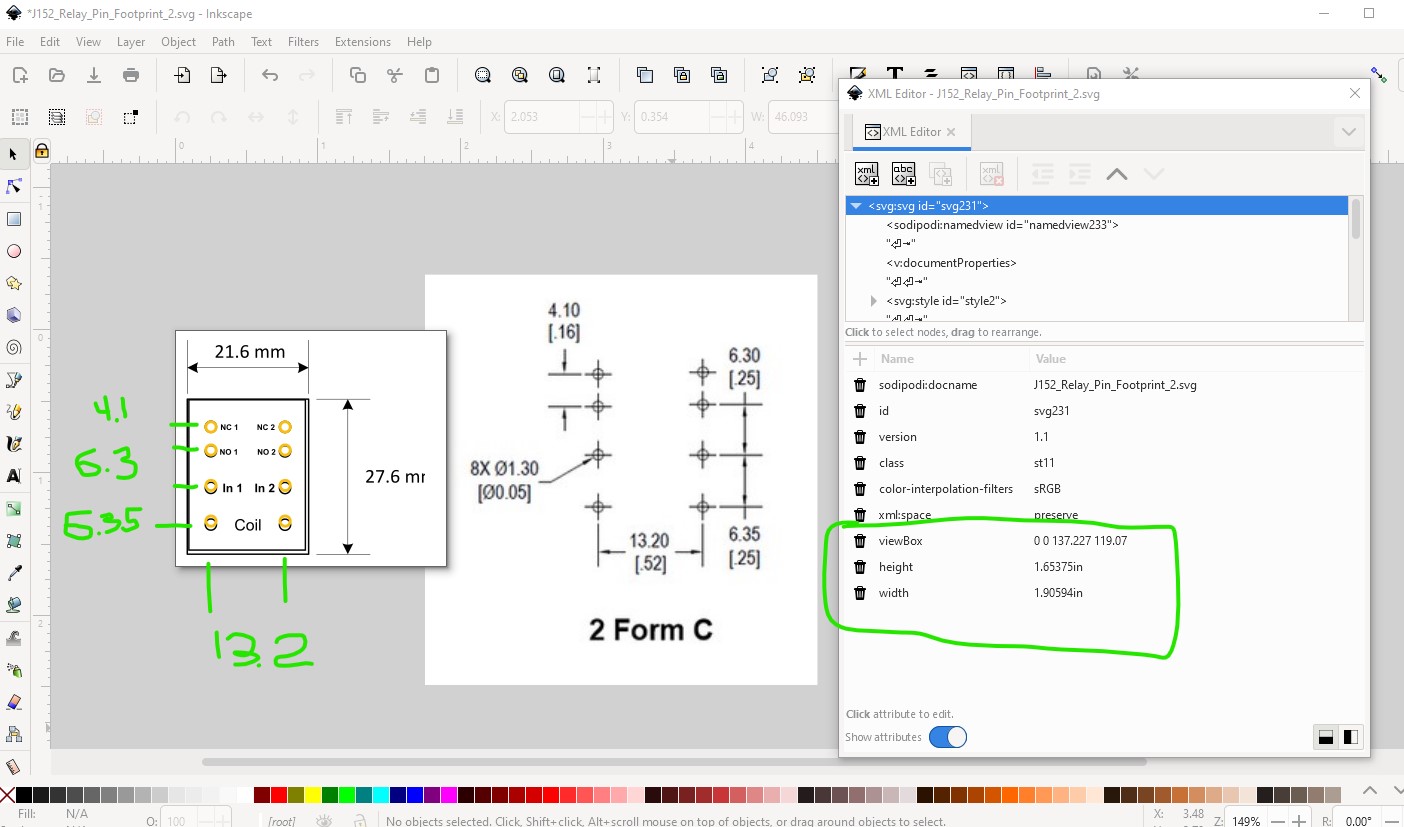
Easiest solution is likely to zip the svg files (the forum is now checking it is a zip file ) and upload them as a .fzpz file. The forum is likely complaining about the height and width parameters (circled in green here) being missing.
That also means the dimensions of the svg won’t be correct, so I would need the dimensions in inches or mm between two points (such as the red arrows in the image) so I can rescale it correctly. Preferably from the start of leftmost pin to the start of the right most pin for maximum accuracy.
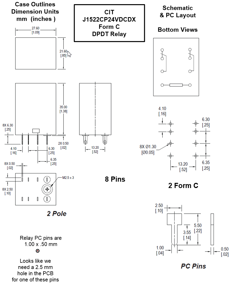
It appears as though this worked. This drawing has dimensions indicated on the drawing. However for completeness sake the footprint is 27.6 mm by 21.6 mm
Yep that worked. Your svg has dimensions (and Visio extensions) so I’m not sure why the forum wouldn’t upload it (maybe the Visio extensions I guess.) While my pcb matches the datasheet, it looks like the data sheet is incorrect.
Here I loaded your svg and overlayed my original pcb on it (the gold pads.) They look to be slightly off in y and the hole is a fair bit too small. I lost the 50/50 chance and the NO and NC pins are reversed as well. In any case I’ll replace the part above (which you will need to delete from your mine parts bin and then restart Fritzing to be able to load the new one!) with a corrected version that looks like this (again my pcb overlaid on you svg)
Peter: Thank you for sharing all of your experience to solve the problems related with updating and correcting this relay circuit model. Your updated circuit drawing for the circuit model in the Schematic Window looks fine.
However, I am curious. Why did you remove the lettering on the circuit model in the PCB Window?
If it is in the part, to remove it the user needs to modify the part (which isn’t simple.) Text can be added to the part in the sketch (without having to modify the part) so the recommendation is to not put text in pcb of a part and let the user add the text if they want it in the sketch.