Hi there,
I make my first PCB in Fritzing.
when try to engrave it with routing machine. I am stuck on ground copper fill trace converting.
It is make out of several small piece of polygons. each of it supposed to overlap each other to form the whole grounding plane.
turn out there are small gaps Between them, make it not possible to be engraved.
what am I doing wrong?
Hi Gabe,
Can you explain a little bit more what the exact issue is?
The image don’t tell anything to people who don’t use that software.
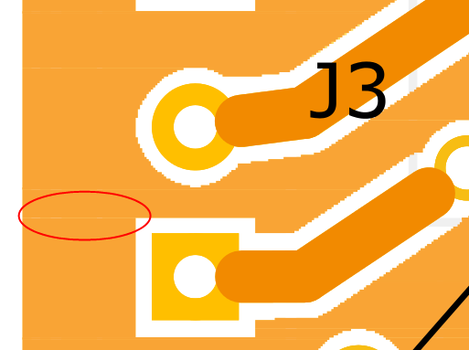
I believe this is a bug  issue; when applying a copper fill, there are small line that are running horizontal from the edge of the ground fill keepout. I did not think they caused a problem… but apparently they do… at least is some cases… My concern is, when you have a board made at a fab house, does your board come back with one continuous ground plane or a bunch of small ones? Could one section of ground plain be totally isolated from the rest of the ground plain? Or are they to small to cause a problem… It looks like it may have something to do with the scan process when creating the ground fill.
It defantly a bug which make Fritzing completely useless for me.
I am not sending it to fab. I want to make it at home with a CNC router.
One dirty fix is to trace back from image.
Does anyone working on this bug out there?
I’m not a dev, I have no idea if someone is on top of this.
BTW what software do you use for the CNC? Could the bug eventually live there?
And why not etch it? Just as messy, less noise, less energy. Allthough seeing a CNC at work is actually entertaining. And you need a laserprinter.