OK, I just tried to duplicate a KiCAD project I put together recently. Creating the schematic and breadboard views were not too hard. The UI does need some serious work, partitularly when disambiguating what a mouse click refers to (one needs to be overly precise when drawing wires in the schematic view – there is ambigiousness between moving parts and drawing wires).
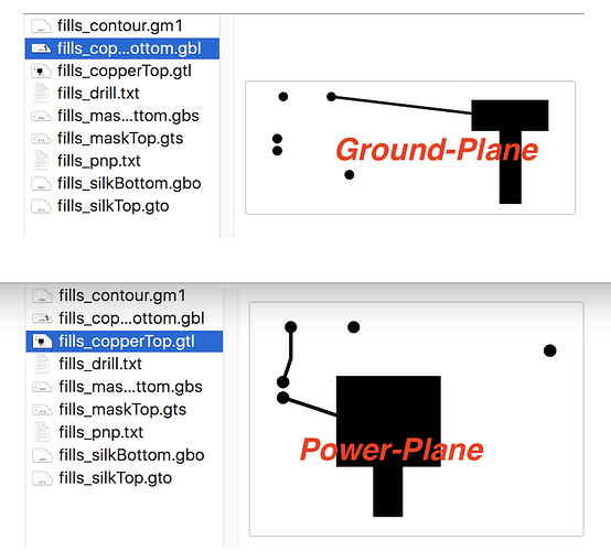
The PCB design view is a total disaster. The circuit I designed uses three I2C breakouts from Adafruit connected to a TTGO-T1 (an ESP32 Devkit clone, available from China for $5/each). There are exactly 4 nets: SDA, SCL, +3v3, and GND. My KiCad design uses copper fill areas for the power and ground busses: the top layer for +3v3 and the bottom layer for GND. There are really only two “routed” nets: SDA and SCL. It was an excessive amout of effort to get those two runs done. Then I discovered that it does not appear to possible to do a copper fill area for power on one side (top) and a ground fill area for the other side (bottom). At that point I gave up. I have designed far more complex boards with KiCAD – Fritzing is far harder to use than KiCAD. The only thing Fritzing brings to the table is the Breadboard view. (And the fact that Adafruit has a zillion parts as Fritzing objects, but I think I will write a Tcl/Tk program to convert Fritzing fxpz files to KiCAD .lib (schematic) and .mod (footprint) files.


