I am very new to designing PCBs, I am creating a custom PCB board shape in Adobe Illustrator. In my illustrator file I have all of the places where I need copper ring holes on the circuit board to go for mounting an Arduino Nano and a few other things. I have imported the board into Fritzing (with the board and silkscreen layers), my question is how do I know where the copper ring holes should go on the board? How do I connect the holes together with a path? Do I just have to drag and drop dozens of holes over where I’ve marked them in Illustrator?
You only need Illustrator (or Inkscape) to create or edit parts. There is an Arduino nano part in core parts (and you can sometimes find parts that aren’t in parts by doing a google search of the form “fritzing part part-name” where part-name is the part you need. That said, drag the nano from the arduino section in to breadboard, along with a led and resistor and connect them up:

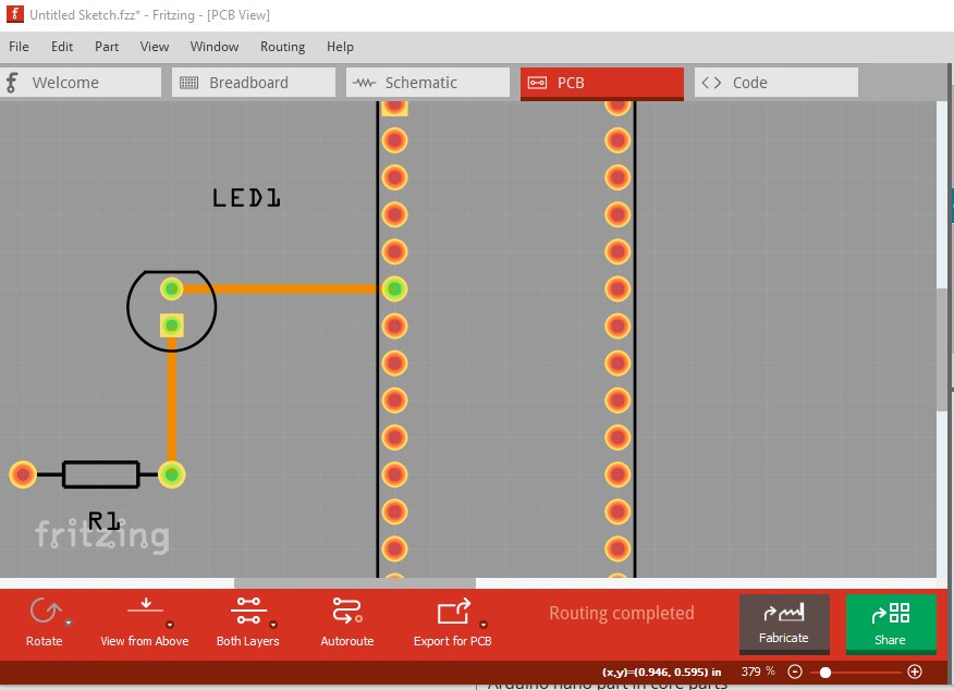
Then switch to pcb view where the connections in breadboard appear as rats nest lines:
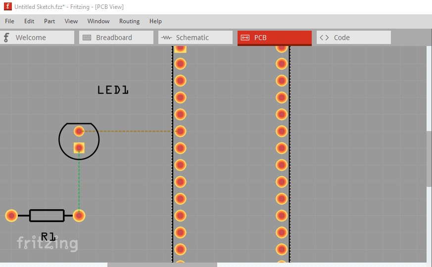
click and drag on a rats nest line and it creates the trace (you can also click on a pin in pcb and create a trace to another pin)
this is all in the documentation.
Peter
I think the original question was about a custom PCB shape, and getting creating mounting holes in the right sizes and places.
It takes some work, but it is possible to create holes in the custom board shape. I do not know a way to have those plated through though. So the general answer is to use the “hole” object provided by Fritzing core library. You can include silk screen guide marks so show where the holes need to go.
You said “dozens of holes”. You should not have that many added holes. Are these the connections, not mounting holes? If so, parts with through-hole connects placed on the board include the holes. They can also include mounting holes, but that is less common.
What did you mean about “connect the holes together with a path”? mounting holes do not need connecting. Part connection points are connected using traces. Examples shown in Peter’s answer.
Thanks for the quick reply. I added some parts but there are some copper ring holes I need in exact positions. Do I just use the silkscreen for this and line them up? When the PCB board is produced does anything from the silkscreen get printed onto the board? Thanks.
Many of the copper ring holes I need are for connected wires from the battery and there are a few buttons which contain a shape I haven’t been able to find in the parts selector. My next question would be in Core Parts > PCB View, do I use “Hole” or “Via”? By path I meant traces, sorry for the confusion. If I place a single hole how do I connect it to, for example, one of the Arduino Nano pins?
Your best bet is probably the hole part in core parts pcb. You can position it via Inspector (the lower right window) where every you need it. It is common practice in parts to put the mounting holes on the silkscreen layer. If the doesn’t want the mounting holes, they do nothing. It they do want mounting holes they drag a hole in to the sketch so the hole will be drilled. It the hole is set in the part (which is possible to do), the user has to modify the part to not have the hole. You can do the same thing here.
Yes, typcially everything on the silkscreen layer will be printed in paint (color selectable on order usually) on the board. In the case where a mounting hole is drilled, the paint disappears (I expect it is still printed, there just isn’t anything for it to stick to!) Before ordering boards it is a good practice to export the sketch as a gerber file and check the gerber output with a gerber viewer (I use gerbv from the geda project, but there are lots of them!) The gerber export happens after pcb view and sometimes things will be different (missing holes in parts due to an error in the part for instance) when it looks fine in pcb view.
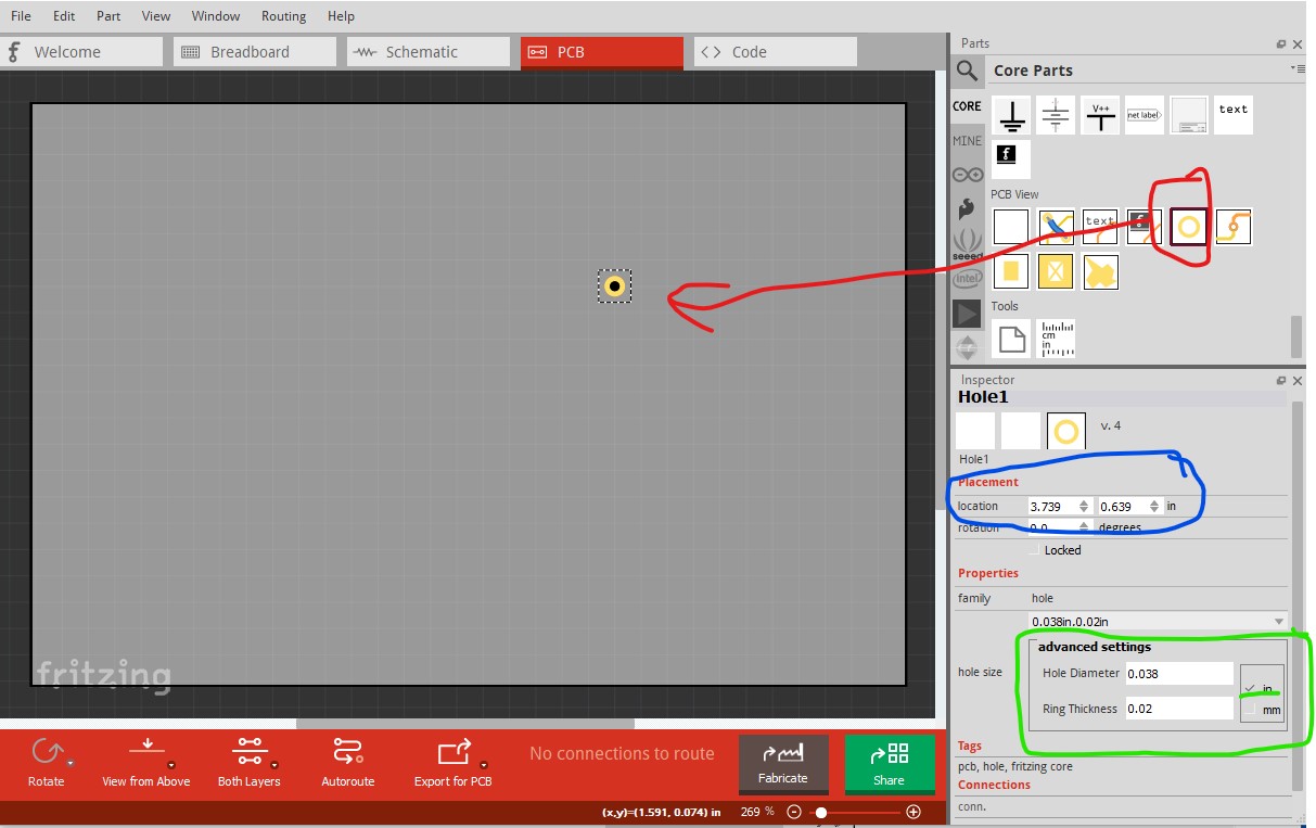
Here I have selected a hole and dragged it in to the sketch (red outlines.) I can change its x/y position via the location (blue outline) and set the parameters of the hole. This is set for a .1 header connector, 0.038in hole size with a 0.02in ring thickness. Setting the ring thickness to 0 will give you a non plated through hole. With the ring thickness non zero you can attach a trace to the pad as with any other part.
By “which contain a shape” do you mean a non circular hole? Fritzing (and I believe most of the cheap board makers) has trouble with slots in PCB. For odd shaped copper pads, your best bet is to make a part and use a path that describes the odd shape over what amounts to a hole (a circle with a stroke-width) in the xml. The gerber export code only cuts holes with a circular pad (or a circular path with no other shape) but will overlay that with a path that describes an odd shape.
Peter
By “which contain a shape” do you mean a non circular hole?
I meant the actual positioning of the holes on the part. I have a couple buttons that I can’t find in the parts and I need the holes in an exact position so I assume I should just place holes where they should be and trace them to the Arduino.
That will work, but what may be better is to modify an existing switch part to have the desired pcb footprint. That way you have breadboard and schematic views rather than only pcb. If you have a pointer to the switches you need, I can make parts fairly easily.
Peter
It’s the RB and LB buttons in an Xbox controller, I’m not sure of the name of the part.
Then I expect the layout of the foot print (x/y coord for each pad, and pad hole size) and the layout of the switch (spst etc) and a picture to make a breadboard image for it would probably be easiest.
Peter
Ok, thank you for your help!