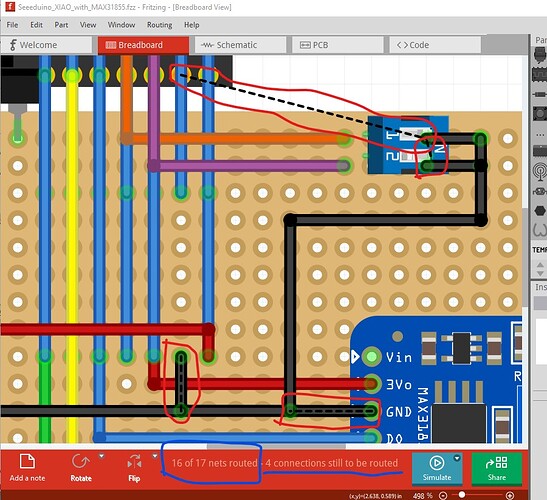
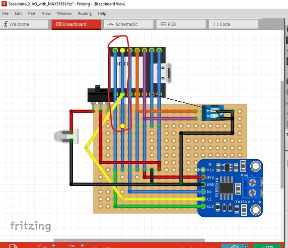
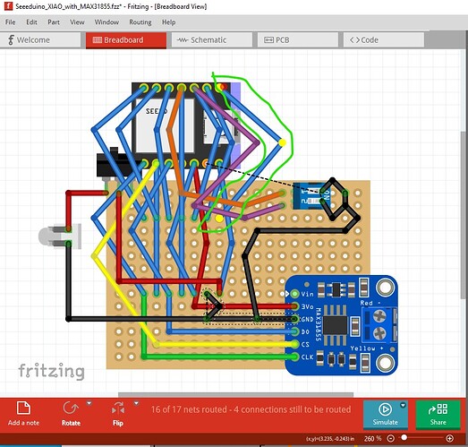
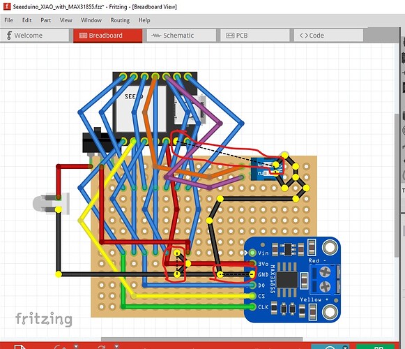
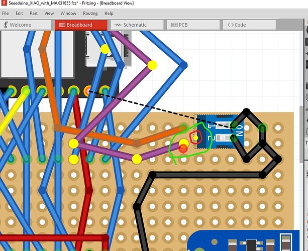
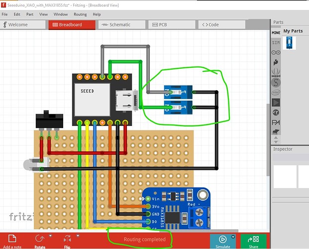
There are a fair number of things wrong here. Lets start with breadboard which is a mess. First is is not correctly routed, which means pcb and schematic may not be correct. at the bottom you see there are 4 unconnected nets. They are outlined in red (each has a rats nest line showing where the connection should go.)
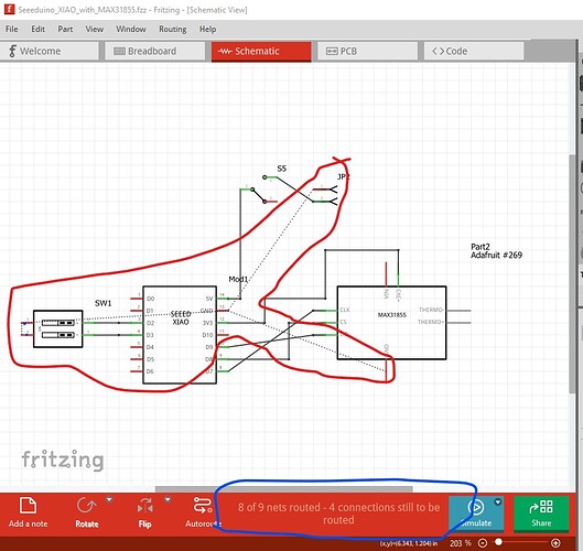
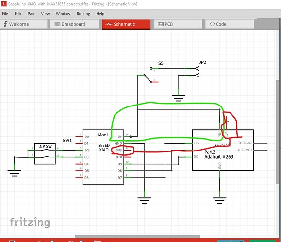
same with schematic, with the same implications, possibility of errors. In this case none of the grounds are connected.
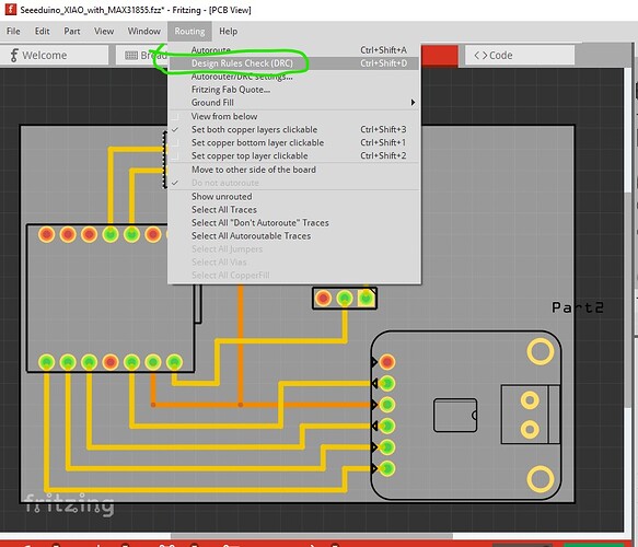
pcb appears to be mostly correct. To verify that run DRC like this, select DRC and left click to start it.
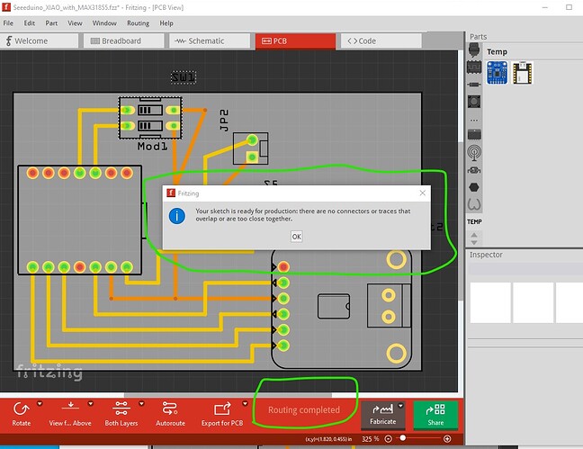
which checks and indicates it didn’t find any errors (that doesn’t mean the board is correct, just that there are no obvious errors present.)
So lets go clean up breadboard. Here I dragged the yellow wire to the left to expose the wire under it, then right clicked on the top pin connected to the blue wire. That lights everything connected to the wire in yellow. Here we see there is nothing connected to it so this wire can be deleted as not needed. That is ends with yet another blue wire going past it indicates more problems.
so drag all the wires apart so we can see the unconnected wires and delete them. There are a lot of them all doing nothing except cluttering up breadboard.
Here I right clicked on a ground pin and it lights everything that should be connecting to ground (even the ones without wires but with rats nest lines) yellow.
here we are looking at the 2 position dip switch (which is broken and needs replacing.) While the connection is showing as there, the wire doesn’t actually connect to the switch (but is close enough to make a connection!)
here is breadboard with all the unused wires removed and the dip switch replaced with 2 correct single pin ones (I eventually made a correct 2 position dip switch and replaced these two with it.) You see that routing is complete at the bottom of the screen. You can also see clearly where each wire goes which is vital to get the wiring correct.
this sketch is your original circuit as wired but without the last error (explained below) corrected. Here I reduced the size of the pcb as far as possible to save weight. Even more can be done if required.
Seeeduino_XIAO_with_MAX31855-fixed.fzz (40.5 KB)
Now this is schematic completely routed with the final error corrected. That error is that the 3.3V pin on the MAX31855 module is an output (from an on board voltage regulator) not an input. The board is expecting 5V on the VIN pin to power the internal regulator to produce the 3.3V that they need for the themocouple or the thermocouple chip. It may work successfully with the original layout because without any connection to VIN the voltage regulator will be inactive, but the external 3.3V connection may introduce noise and make the readings less accurate, that is likely the purpose of the local voltage regulator. Here I connected VIN on the MAX board to the 5V input as they intended and disconnected the wire to the 3.3V output from the XIAO (since that would conflict with the now active 3.3V regulator on the MAX board.)
That is contained in this sketch.
Seeeduino_XIAO_with_MAX31855-corrected.fzz (40.8 KB)
If you are comfortable soldering the XIAO as an SMD chip you can use the XIAO SMD version of the part available here:
That would allow you to solder it directly to the pcb saving the weight of the headers otherwise required to attach to it (although soldering wires in will also work to eliminate the connectors.) Hope this helps!
Peter
