I’m looking for some feedback on my first PCB design.
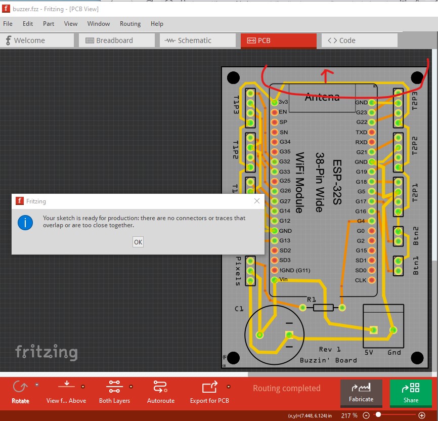
This design passes the DRC, but I’m not sure how reliably that translates into a good fabricated board.
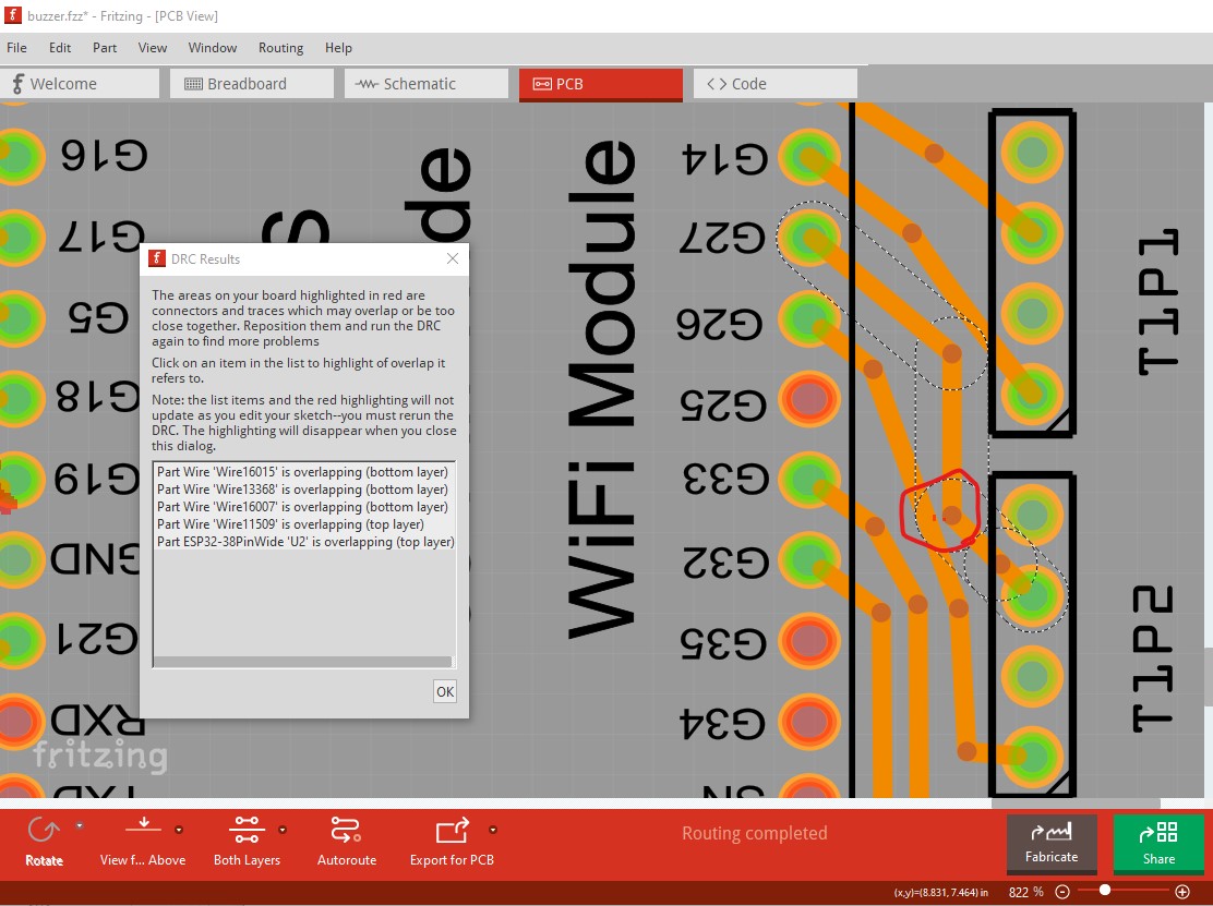
Are the mount holes too close to the edges?
There are a couple of traces overlapping the labels from the esp32 board. Is that ok?
Any feedback on how to power an ESP32 board from a 12V wall power supply would be great. I currently plan on using a DC-DC buck converter I have lying around. It’ll connect to the screw terminals. It’s working fine on the breadboard setup. Is there anything else I should be doing?
Any other general feedback would be great. This is the first time I create a PCB design to send out for fabrication.
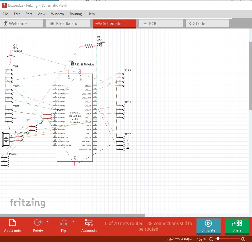
Yes the text is on silkscreen layer and will be applied over the traces (which are covered by solder mask although silkscreen isn’t usually conductive anyway.) That said, I would advise routing schematic and checking that all the connections you expect appear in schematic. In PCB I would move the circled trace up a bit. It is close to the keepout area on the antenna and you have space to move it up. A trace can act as a short across the antenna and affect reception.
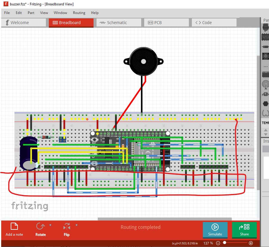
It looks to me like you are missing this wire in breadboard which has the effect of disconnecting the pins connected to the bottom from power. This is where routing schematic helps you would see the lack of expected connections (hopefully) in schematic.
clicking on a pin on the top power bus lights yellow everything connected to it. As you see the bottom power bus has no connections (although that may be intentional for some reason) but is suspicious. The headers on the bottom will not connect to the power on the top which as noted may or may not be what you intend. This will reflect in to pcb view as well and make the pcb incorrect if it isn’t intended. Schematic isn’t currently routed which would also show this if it was routed.
It looks like the bottom bus may be 3.3V and the top 5V which means this may be working as expected. From the pixels label if you are using pixel LEDs they can require more current than you expect. The driver chips are asynchronous so you need to size the power supply to be able to supply the peak current used by all pixels drawing their maximum current at the same time (which will happen occasionally and can cause a power supply collapse if not expected and allowed for.) Other than that it looks fine.
You guessed right. Some of the circuitis 3.3V and some 5V. Only the esp32 and the LEDs are powered by 5V. The rest of the circuit is the esp’s required 3.3V logic level.
There are only 16 LEDs on the pixel strip so I’m not concerned with power for them.
TIL about antenna keep out area. Is it simply the box on the silkscreen? Is that still a keepout for traces on the other opposite layer of the board?
I reworked it to include a buck converter board and all of your feedback. buzzer.fzz (69.1 KB)
Other than that you need to make sure the buck converter pcb footprint is correct, usually by printing it out at 1:1 scale and comparing the holes to a real part (if you are using the actual part described by the Fritzing part this is still worth doing before ordering boards!) Another good bet is to check the drill.txt gerber file to make sure the holes for all parts are big enough. Some parts have pcb holes that are too small (especially ones obtained from the net, although there are some in core parts as well.)