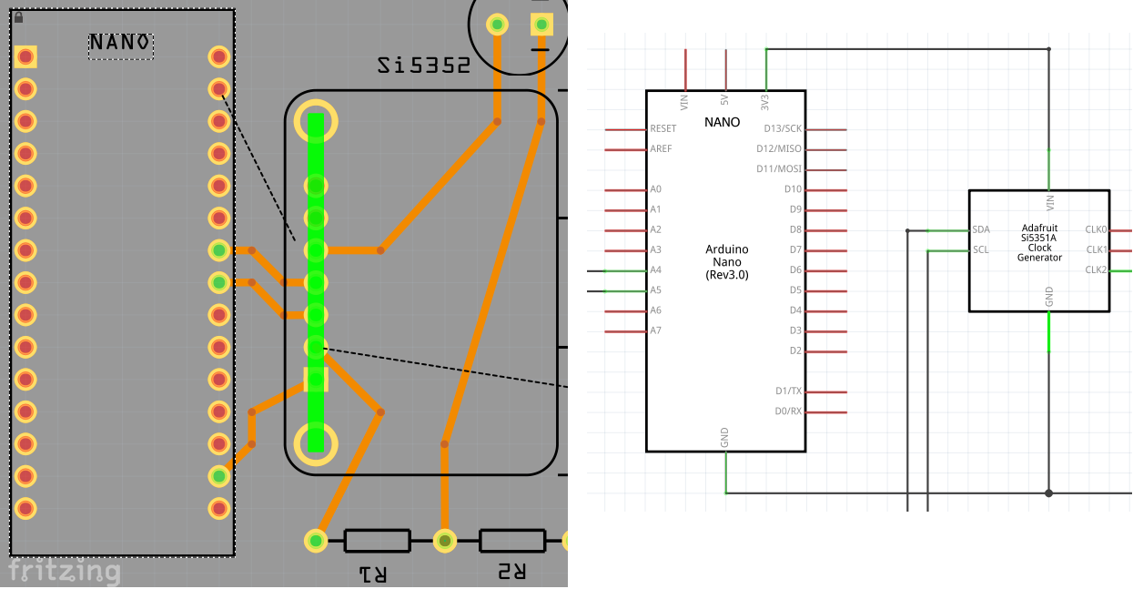
Connected GND pin from Arduino NANO and GND pin on Si5351. Looks good on the schematic but on the PCB the pins are not connected. GND from NANO just floats and is not connected to Si5351.
What I expected should have happened instead:
Should have gotten connected properly.
My version of Fritzing and my operating system:
Windows 10. Version 0.8.7
Please also attach any files that help explaining this problem
My first guess is going to be a broken Si5352 part. Also is your Fritzing version really 0.8.7? Current version is 0.9.4. In any case if you would post the .fzz file for the sketch that produced the pictures above (which will contain the custom part) I’ll have a look at what may be wrong. Upload is the 7th icon from the left in the reply menu.
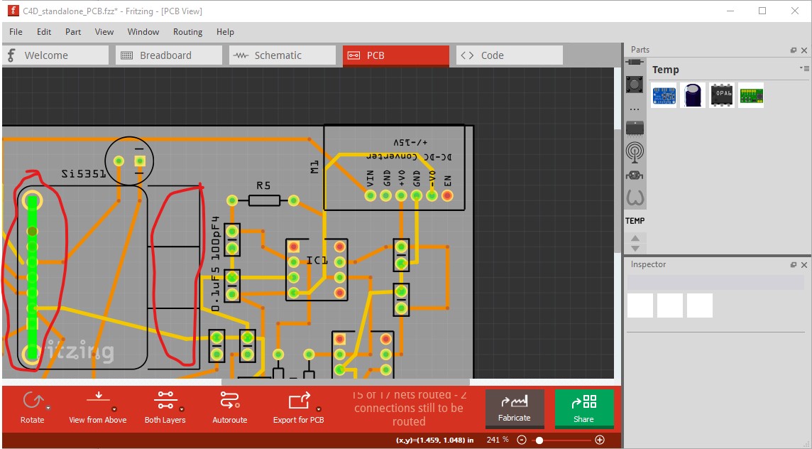
I see the same issue with connecting +15V and -15V from the boost converter C4D_standalone_PCB.fzz (75.0 KB) to pins 7 and 4 on IC2 – the schematic looks fine but the PCB connection doesn’t exist. Please see attached for the fzz file.
I see ratsnest wires (dashed lines) on the PCB view in the uploaded fzz file. That is what is expected. Creating a connection in one view places a wire there, and a straight ratsnest line between the matching nets in other views. It does not create a wire in other views. To create the wire, double click on, or drag the middle of, the ratsnest line. Then finish routing (bending, moving) the now ‘real’ wire to fit where you want. Nets are sets of connections that Fritzing believes are connected together, either by actual wires, or ratsnest lines.
When I created the ground connection, the wire did not end correctly on the Si5351 connection point. That is probably the broken part that @vanepp mentioned. I did not look at the part details. The -V0 wire looked correct, once created from the ratsnest line.
@microMerlin, I haven’t converted the ratnest wire to a connection wire yet because it is on the wrong pin – I had made the connection earlier and checked from the bottom and the top – still looks wrong. Thanks for your input, though.
@vanepp, I downloaded a newer version of Fritzing. Thank you for taking my brain out of the 2014 version. Although, I still see the same problem. So I think it is a broken Si5351 (Not Si5352 as seen in the first post, I have corrected it in the .fzz file I uploaded for your reference). How do I fix a broken part? What exactly is “broken?”
Indeed the Si5351 part appears to be pretty broken. It looks like they used Eagle2Fritzing, but didn’t do the necessary clean up of the part, I’m not immediately sure what exactly is broken as there are a large number of reported errors, but I am familiar with fixing up Eagle2Fritzing parts as I often use it to make parts. Unless you are familiar with part creation, it is probably easier if I fix up the part. It will probably take me until tomorrow some time.
@vanepp, yes please! I am unfamiliar with Eagle2Fritzing conversion, I am still new to this. Did you also see how the +V0 and -V0 from the dual boost converter are not getting connected to pins 7 and 4 respectively on the second IC? Thoughts? Thank you so much!
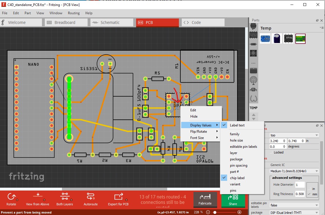
The circled green bar on the SI5351 shouldn’t be there, and there should be three clock output pads in the area of the empty red circle on the end of the si 5351 part (although since they are smd pads they may need wires added to work.) In order to connect -VO on the converter you need to click and drag on the rats nest line (circled in red here) which will create a trace on the bottom of the board. You then need to right click on the trace and select move to top layer to get it to the top layer and route it to the pin on the converter to create the image above.
I am not using the padded terminals on Si5351 to get the clock output. I’m using the pin labeled “2” on it. The padded terminals are just there, occupying my circuit board space, haha.
And yes, I can see IC1’s pin 4 connected to -V0. I am referring to the 8-pin IC right below it. It is missing the part label, it should be IC2 (OPA606 on the schematic).
Ah! I had missed that the clock pins come out on the header as well. That makes things easier. A note going by, you probably want to add two resistors across the +V and -V outputs of the boost regulator. As you will see in the description of the part, for good line regulation there needs to be a minimum 20ma load on the switcher and they recommend adding load resistors if your load is less than 20ma (which it may be in this case.) Also if you need very low noise it would be a good idea to use the ±24V version of this (or another, I made a number of these parts and I think only one had a +/-24V version ) and follow it with a 78L15 /79L15 linear regulator pair to get a lower noise 15V supply.
Right click on the part label (the red arrow in the image) and select display values and you can select what to display:
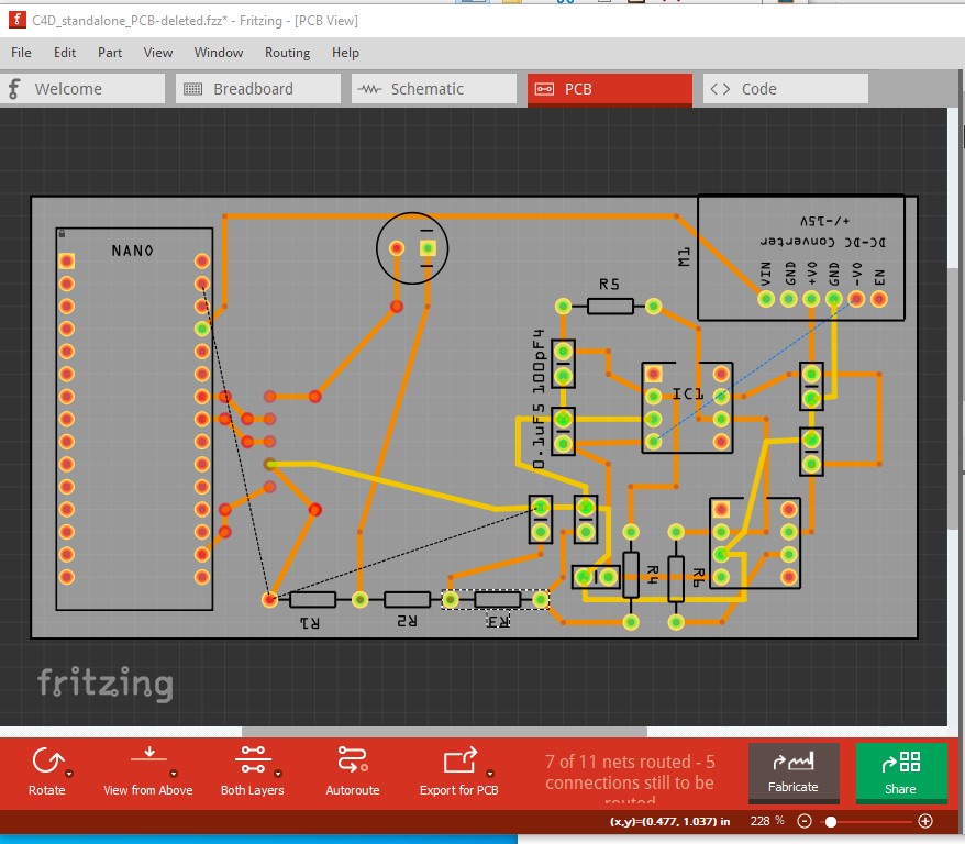
using this is a bit complex. First you have to delete the old part and then save the sketch and exit Fritzing for the old part to be completely deleted. The easiest way to do that is to select the Adafruit part then right click on it and select “delete minus”. This deletes the part but leaves the traces that connect to it in place and produces this:
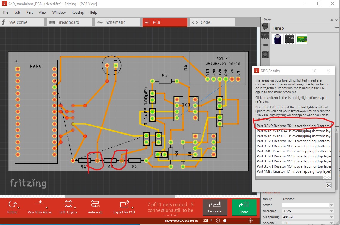
the adafruit part is gone, but the traces connecting to it remain. If the Adafruit part is in your mine parts bin, you need to select it in the bin then right click and hit delete. Unfortunately due to a bug, that doesn’t actually delete the part, to do that you need to exit Fritzing (at which point it does completely delete the part) then restart Fritzing. At this point you can load my new Adafruit part above and drag it in to the sketch. Once it is placed, you need to click on the end of each trace in turn and drag it to the correct connector on the Adafruit part until the connector turns green to indicate a successful connection. It is sometimes easier to just delete the trace and re route it though. The second problem is with the three resistors, R1 - R2 -R3. Their holes are overlapping (as DRC, routing->Design Rules Check shows us):
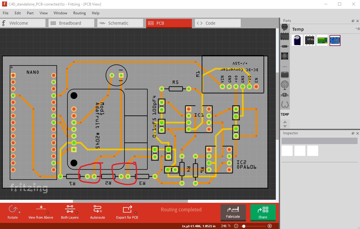
and click and drag to create traces that connect the pads to each other. I have also loaded my new part and redone the connections and now we see that routing is complete, and DRC is happy with the sketch.
as well pcb best practice is for all traces to come out of a pad at a 90 degree angle and make turns at 45 degrees (not 90 degrees.) I did some of but not all of that here. You sometimes need to decrease the default grid size from 0.1in to something like 0.05in to achieve that (although I didn’t do that here.)
Peter, you’re a life saver! Thank you very much! The ground is connecting to the required terminal now. And thank you for the tips on good PCB design practices. I will incrorporate them.